
CID Certification: Learning the “Why” Behind PCB Design Requirements
Jun 04, 2026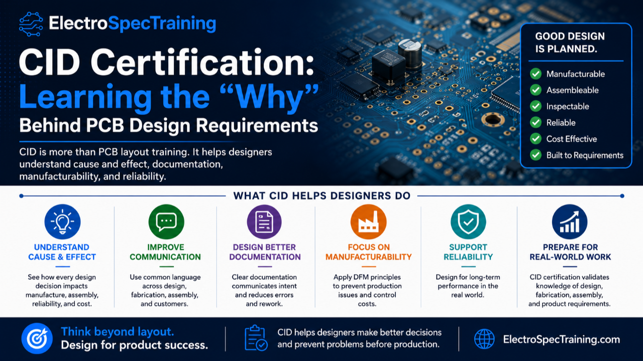
CID Certification: Learning the “Why” Behind PCB Design Requirements
PCB design is much more than knowing how to use layout software.
Many people think PCB design is simply placing components, routing traces, setting up layers, and generating fabrication files. Those skills matter, but good PCB design goes much deeper.
A strong designer must understand how design decisions affect fabrication, assembly, inspection, reliability, cost, and long-term product performance.
That is where CID training becomes valuable.
CID is not just PCB design training.
CID is design decision training.
It helps designers understand why requirements exist, how they connect to real manufacturing outcomes, and how small layout choices can create major downstream problems.
PCB Design Is More Than Layout Software
PCB design tools are powerful, but software does not make engineering decisions for you.
A layout tool may allow a design choice, but that does not mean the choice is manufacturable, inspectable, reliable, or cost-effective.
CID helps bridge that gap.
It teaches designers to think beyond the screen and consider what happens when the board moves into fabrication, assembly, test, inspection, and field use.
A designer needs to understand materials, stackup, conductor spacing, hole tolerances, annular ring, via structures, land patterns, documentation, fabrication notes, assembly requirements, and product class expectations.
Those decisions determine whether a design is easy to build, difficult to build, expensive to build, or risky to build.
CID Helps Designers Understand Cause and Effect
One of the biggest values of CID training is that it teaches cause and effect.
A PCB design decision may look small in layout, but it can create serious problems later.
Insufficient annular ring can affect hole reliability.
Poor conductor spacing can create electrical or manufacturing risk.
Weak stackup planning can affect impedance, return paths, EMI, and signal integrity.
Incorrect land pattern selection can create soldering defects.
Bad via placement can affect manufacturability, reliability, and rework access.
Missing fabrication notes can create confusion between designer, fabricator, assembler, and inspector.
Unclear class requirements can result in product being built or inspected to wrong expectation.
CID helps designers understand that each design decision has consequence.
Good PCB design is not just drawing copper.
Good PCB design is controlling risk before product reaches production.
CID Builds Better Communication Between Design, Fabrication, and Assembly
PCB design is not done in isolation.
The designer communicates with fabricators, assemblers, inspectors, engineers, quality teams, purchasing teams, and customers through documentation and design intent.
CID gives designers common language with these groups.
When everyone understands requirements, design intent becomes clearer. Fabricators know what needs to be built. Assemblers understand how product should be assembled. Inspectors understand what criteria applies. Quality teams understand what was specified and why.
This reduces confusion.
It also reduces rework, delays, supplier questions, and production surprises.
Many manufacturing problems are not caused by lack of effort. They are caused by unclear requirements, poor communication, or design decisions that did not fully consider downstream impact.
CID helps close that gap.
Documentation Is Part of the Design
A PCB is not fully defined by layout files alone.
Fabrication drawings, assembly drawings, notes, tolerances, material requirements, plating requirements, class requirements, surface finish, solder mask, legend, stackup, controlled impedance, hole tables, and special instructions all help define product.
CID reinforces that documentation is part of design.
A well-routed board with poor documentation can still create problems.
If requirements are missing, vague, inconsistent, or not properly flowed down, suppliers may make assumptions. Those assumptions may not match design intent or customer expectations.
CID helps designers understand what needs to be communicated and why it matters.
Why On-Demand CID Training Makes Sense
CID covers a large amount of technical material.
It is difficult to absorb everything in a fast classroom setting. PCB design requirements build on each other, and students often need time to review concepts, revisit weak areas, and connect lessons to their own experience.
That is why on-demand CID training is such a strong fit.
With on-demand training, students can pause, rewind, rewatch, and study at their own pace. They can spend more time on areas where they need help and move faster through areas they already understand.
This is especially important for design training because the material is not just procedural. It is conceptual.
Students need time to understand why requirements exist and how they affect real product.
A strong CID program should include recorded instruction, study guide material, practice questions, and exam preparation. But more importantly, it should help students build design judgment.
CID Certification Shows Breadth of Knowledge
CID certification does not mean someone becomes a perfect PCB designer overnight.
No certification does that.
But CID does show that a designer has been exposed to broad design concepts, documentation requirements, manufacturability concerns, material considerations, land pattern principles, via structures, stackup planning, fabrication requirements, assembly impact, and reliability concerns.
That breadth matters.
A designer who understands only layout mechanics may complete a board, but a designer who understands design requirements can help prevent problems before they happen.
CID gives designers a stronger foundation to make better decisions and ask better questions.
CID Is Especially Valuable for Designers Moving Into Higher Responsibility
CID is useful for new designers, but it is also valuable for experienced designers who want stronger technical foundation.
As designers move into more complex products, higher reliability applications, tighter tolerances, controlled impedance, dense routing, flex, rigid-flex, HDI, RF, aerospace, defense, medical, or Class 3 work, design decisions become more critical.
Small mistakes become more expensive.
Unclear requirements create bigger risks.
CID helps designers understand how to think more systematically about requirements, documentation, fabrication, and assembly impact.
It helps move designers from simply completing layout to designing for product success.
Bottom Line
CID certification is not just about passing an exam.
It is about understanding why PCB design requirements exist and how better design decisions prevent manufacturing, assembly, inspection, and reliability problems.
CID helps designers think beyond layout software.
It builds common language between design, fabrication, assembly, inspection, and quality.
It strengthens documentation.
It improves understanding of cause and effect.
It helps designers make decisions that support manufacturability, reliability, and product performance.
In simple terms:
PCB layout software helps designers create board geometry.
CID helps designers understand what that geometry means.
That is why CID is valuable.
It helps designers stop thinking only in terms of layout and start thinking in terms of product success.
Want to strengthen your PCB design knowledge and prepare for CID certification? ElectroSpec’s CID training helps designers understand the “why” behind PCB design requirements, documentation, manufacturability, and product reliability. Visit us at www.ElectroSpecTraining.com
