Component Technologies and Why Package Selection Matters
Sep 18, 2026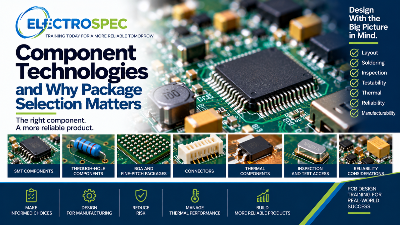
Component selection is not only an electrical decision.
It is also a PCB design decision, manufacturing decision, inspection decision, test decision, thermal decision, and reliability decision.
A component may meet the schematic requirement but still create problems in layout, soldering, cleaning, coating, inspection, test, rework, or field performance.
That is why PCB designers must understand component technologies.
The package matters.
A Component Is More Than a Symbol
In a schematic, a component may appear as a symbol with pins and values.
On the PCB, that component becomes a physical object with a package, body size, terminations, height, mass, orientation, thermal behavior, and manufacturing requirements.
Designers should consider:
- package type
- termination style
- pin pitch
- component height
- component mass
- thermal pad requirements
- soldering process
- inspection visibility
- rework access
- connector loading
- environmental exposure
The schematic identifies the function. The layout must support the physical component.
Package Selection Affects Layout
Different packages create different layout needs.
A through-hole component affects hole size, annular ring, lead fit, solder fill, and board thickness.
An SMT component affects land pattern, solder paste, placement, reflow, inspection, and rework.
A BGA affects fanout, via strategy, X-ray inspection, test access, and routing density.
A connector affects mechanical support, mating access, retention, cable strain, and service use.
A high-power component affects copper, heat spreading, thermal vias, and board temperature.
Package selection changes the design problem.
Solder Joint Formation Depends on the Package
The component package affects how solder joints form.
Designers should understand how package selection influences land patterns, pad geometry, thermal relief, solder volume, wetting, component alignment, inspection criteria, and rework.
The soldering operator forms the joint, but the designer creates many of the conditions that make a good joint possible.
A poor land pattern or poor package choice can make good workmanship difficult.
Inspection Access Depends on the Package
Some packages are easy to inspect visually.
Others are hidden or partially hidden.
Bottom termination components, BGAs, QFNs, and dense packages may require X-ray, process validation, test coverage, or alternate verification methods.
Designers should ask:
- Can the solder joints be inspected?
- Are markings visible?
- Can polarity be confirmed?
- Is X-ray needed?
- Can the product be tested if the joint cannot be seen?
Inspection access should be considered before package selection is finalized.
Testability Depends on Package and Placement
Component selection affects test access.
Dense packages may consume routing area and reduce access to test points. Fine-pitch parts may require boundary scan or other test strategies. Connectors may be needed for programming or functional verification.
Designers should consider testability before layout completion.
A product that cannot be tested effectively may be difficult to accept with confidence.
Thermal Performance Depends on Package Choice
Components generate heat differently.
Some packages rely on leads, pads, exposed thermal pads, copper pours, thermal vias, heat sinks, airflow, or enclosure conduction.
Designers must understand the package thermal path.
A thermal pad without proper copper and via support may not perform as intended.
A high-power component placed poorly may affect nearby parts, solder joints, or product life.
Thermal behavior should influence component placement and layout.
Mechanical Reliability Depends on the Package
Some components are more sensitive to mechanical stress.
Large components, tall components, heavy components, ceramic capacitors, connectors, relays, transformers, and edge-mounted parts may require special attention.
Designers should consider board flexure, vibration, shock, handling, connector insertion force, cable strain, and support.
A component can be electrically correct and mechanically risky.
Availability and Substitution Matter
Component technologies also affect supply chain risk.
A package may be available today but difficult to source later. A substitute may have different dimensions, terminations, thermal behavior, solderability, or qualification status.
Designers should control approved parts and evaluate substitutions carefully.
For high-reliability products, a component substitution is not just a purchasing action. It may be a design and qualification decision.
Documentation Must Communicate Component Intent
The release package should communicate component requirements clearly.
That includes BOM accuracy, approved manufacturer information, polarity, orientation, placement, special handling, soldering requirements, inspection needs, test access, coating or keep-out requirements, and rework limitations.
A good component choice can still create problems if documentation is unclear.
CID Builds Component Awareness
ElectroSpec’s CID Fundamentals course includes component technologies because PCB designers need to understand how parts affect layout, manufacturability, inspection, test, thermal performance, and reliability.
The course provides 22+ hours of self-paced, on-demand PCB design training across 12 structured modules covering materials, layout principles, mechanical and electrical considerations, thermal management, component technologies, interconnections, fabrication requirements, documentation, quality assurance, manufacturability, and standards-based design thinking.
Final Thought
Component selection is not only about electrical function.
The package affects layout, soldering, inspection, test, thermal behavior, mechanical reliability, documentation, and product acceptance.
A strong PCB designer understands that every component brings physical consequences to the board.
Good component decisions make good products easier to build, verify, and trust.
Related ElectroSpec Training
ElectroSpec’s CID Fundamentals course provides 22+ hours of self-paced, on-demand PCB design training across 12 structured modules.
The course helps designers build a standards-connected foundation in materials, layout, mechanical and electrical considerations, component technologies, fabrication, documentation, manufacturability, quality, and design decision-making while preparing for CID certification.
Coming Next
RF/Microwave PCB Design: Materials, Stackup, and Signal Behavior
In the next article, we will return to the CID Advanced track and discuss why RF and microwave PCB design requires careful control of materials, stackup, copper, impedance, geometry, fabrication, and verification.