
Design It Right the First Time: How IPC CID Training Helps Prevent Costly PCB Mistakes
Jun 16, 2026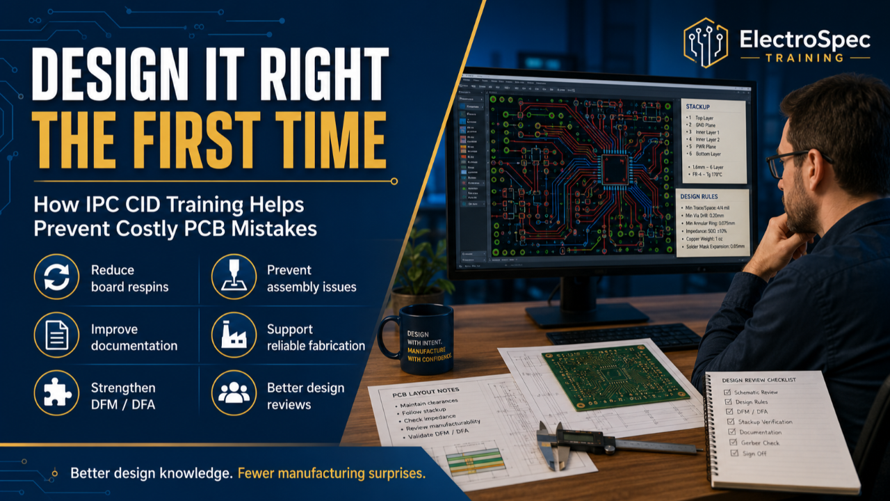
Design It Right the First Time: How IPC CID Training Helps Prevent Costly PCB Mistakes
Every PCB designer wants the board to work the first time.
But in real electronics manufacturing, design mistakes often show up late, after the board has already been sent to fabrication, assembled, tested, or even delivered to the customer.
That is when the cost of a mistake becomes painful.
A missing note, weak land pattern, poor spacing decision, incomplete stackup, inadequate annular ring, poor test access, or unclear fabrication requirement can create delays, supplier questions, board respins, assembly defects, and reliability problems.
IPC CID certification helps designers reduce that risk.
CID training gives PCB designers, layout professionals, and engineers a stronger understanding of how design decisions affect fabrication, assembly, inspection, test, and long-term product performance.
In simple terms:
Better design knowledge leads to fewer manufacturing surprises.
PCB Mistakes Are Expensive Because They Happen Late
A PCB design issue caught during layout review may take minutes to correct.
The same issue found after fabrication may require a new board order.
The same issue found after assembly may require rework, scrap, engineering review, schedule recovery, and customer explanation.
The same issue found in the field may become a reliability problem, warranty issue, or product failure.
That is why designing it right the first time matters.
PCB design is not just about connecting nets. It is about creating a design package that can be fabricated, assembled, inspected, tested, and supported with confidence.
IPC CID training helps designers think through those risks before the board leaves the design environment.
Common PCB Design Mistakes CID Training Helps Prevent
Many PCB design problems are not caused by lack of effort. They are caused by gaps in standards knowledge, fabrication awareness, documentation discipline, or assembly understanding.
CID training helps close those gaps.
Common mistakes include:
- Trace widths or spacing that do not match manufacturing capability
- Inadequate annular ring or hole-to-pad relationships
- Via structures that increase fabrication cost or risk
- Poor component land pattern selection
- Insufficient component spacing for assembly or inspection
- Missing polarity, orientation, or reference designator clarity
- Weak stackup definition
- Unclear material or finish requirements
- Poor test access
- Incomplete fabrication notes
- Incomplete assembly notes
- Design choices that create soldering or rework challenges
- Documentation that leaves too much interpretation to the supplier
Each of these can create delays or defects.
CID training gives designers a more disciplined way to think through those issues before release.
Fabrication Problems Often Start in Design
Fabrication suppliers can build amazing boards, but they still need a design that respects process capability.
If the design pushes minimum features too far, ignores tolerance stackups, lacks clear hole requirements, or uses unclear documentation, the fabricator must stop and ask questions. That creates delay.
Sometimes the supplier can adjust the design. Sometimes engineering must approve changes. Sometimes the board must be redesigned.
CID training helps designers understand fabrication concerns such as:
- Material selection
- Board thickness
- Copper weight
- Hole size and finished hole requirements
- Plating requirements
- Annular ring
- Trace and space limitations
- Aspect ratio
- Layer stackup
- Solder mask registration
- Surface finish
- Controlled impedance
- Fabrication drawing requirements
A PCB designer does not need to be a fabrication shop operator, but they do need to understand how design choices affect fabrication success.
Assembly Problems Also Begin at the Layout Stage
A board can be fabricated correctly and still be difficult to assemble.
Poor land patterns, tight component spacing, unclear orientation, inadequate thermal relief, component shadowing, difficult rework access, and poor panelization can all create assembly problems.
Those issues may not be obvious in schematic review.
They show up when solder paste is printed, components are placed, the board enters reflow, through-hole parts are soldered, or inspectors try to evaluate the completed assembly.
CID training helps designers think about design for assembly.
That includes questions such as:
- Can parts be placed reliably?
- Are land patterns appropriate?
- Is component orientation clear?
- Is spacing adequate for assembly and inspection?
- Can solder joints form correctly?
- Can the board be cleaned if required?
- Can high-risk parts be reworked if needed?
- Is test access adequate?
- Are polarity and markings clear?
- Does documentation tell the assembler what is required?
These questions matter because assembly defects are often blamed on production when the root cause started in layout.
Documentation Is Part of the Design
One of the biggest mistakes in PCB design is treating documentation as an afterthought.
A layout file is not enough.
A complete design package should tell the fabrication and assembly suppliers exactly what is required.
Good documentation reduces assumptions. Poor documentation creates confusion.
CID training reinforces the importance of complete design documentation, including:
- Fabrication drawing
- Assembly drawing
- Stackup requirements
- Material requirements
- Surface finish
- Hole requirements
- Controlled impedance requirements
- Tolerances
- Marking requirements
- Solder mask requirements
- Notes and special instructions
- Applicable IPC standards
- Class requirements
- Revision control
When documentation is incomplete, suppliers must guess, ask questions, or make assumptions.
None of those are ideal.
Designing it right the first time means documenting it right the first time.
CID Helps Designers Reduce Respins
A board respin is expensive because it consumes more than board cost.
It can affect:
- Engineering time
- Supplier lead time
- Assembly schedule
- Test schedule
- Program milestones
- Customer commitments
- Material availability
- Production launch dates
- Team confidence
Some respins are unavoidable. Requirements change. Components become unavailable. Engineering learns from test results.
But many respins can be prevented through stronger design practices.
IPC CID training helps designers reduce preventable respins by improving their understanding of standards, manufacturability, documentation, and design review discipline.
The goal is not perfection. The goal is fewer avoidable mistakes.
CID Supports Better Design Reviews
Design reviews are more effective when the team knows what to look for.
A review that only checks schematic connectivity and basic layout completion can miss major manufacturability risks.
CID-trained designers bring stronger questions to the review:
- Does the stackup support the design requirements?
- Are trace and space rules realistic for the supplier?
- Are holes and pads properly defined?
- Are land patterns appropriate for assembly?
- Is solderability supported?
- Are there inspection or test access issues?
- Are controlled impedance requirements clearly documented?
- Are fabrication notes complete?
- Are assembly notes clear?
- Are IPC class requirements stated?
- Are supplier assumptions minimized?
This kind of review helps catch problems before release.
That is where CID training creates real value.
CID Builds a Common Language Across Teams
PCB design is a team activity.
Designers work with electrical engineers, mechanical engineers, fabrication suppliers, assembly suppliers, test engineers, quality engineers, program managers, and customers.
Communication problems between those groups can create costly mistakes.
IPC CID training helps build a common language around design rules, fabrication requirements, assembly risk, documentation, inspection, and reliability.
When teams share that language, they make better decisions.
A designer who understands manufacturing can communicate more effectively with suppliers.
An engineer who understands IPC design expectations can write better requirements.
A quality engineer who understands design intent can ask better review questions.
A program manager who understands design risk can better protect schedule and cost.
CID helps connect those roles.
Design Software Cannot Replace Design Judgment
Modern PCB design tools are powerful, but they cannot replace standards knowledge and judgment.
Design rule checks are only as good as the rules entered.
A tool may allow a feature that is risky for a specific supplier. It may not understand your fabrication cost target. It may not know your assembly process limitations. It may not recognize that documentation is incomplete. It may not judge whether a design is practical for inspection, test, or rework.
That is why CID matters.
CID training helps the designer understand why rules exist, not just how to enter them into software.
Software can route the board.
CID knowledge helps make the board buildable.
Who Should Take IPC CID Training?
IPC CID training is valuable for:
- PCB designers
- PCB layout professionals
- Electrical engineers
- Product engineers
- Manufacturing engineers
- Quality engineers
- Design reviewers
- Engineering managers
- Technical leads
- Anyone responsible for PCB design quality
It is especially valuable for professionals who want to reduce manufacturing risk, improve documentation quality, strengthen design reviews, and build more reliable printed board designs.
ElectroSpec Training’s IPC CID Course
ElectroSpec Training provides IPC CID certification preparation for PCB designers, engineers, and technical professionals who want practical, standards-based training.
Our CID course is designed for busy professionals who need focused preparation and flexible access.
The course helps students understand the design concepts, IPC expectations, documentation practices, and exam topics needed to prepare for certification.
ElectroSpec’s CID training supports:
- On-demand learning
- Practical exam preparation
- Standards-based instruction
- Study support
- Practice questions
- Instructor support
Whether you are building your first formal PCB design credential or strengthening years of layout experience, CID certification can help you become a more capable and confident designer.
Final Thought
A PCB mistake is easiest to fix before the board is released.
That is why design knowledge matters.
IPC CID training helps designers make better decisions earlier, reduce avoidable mistakes, improve documentation, strengthen supplier communication, and support boards that can be fabricated, assembled, inspected, tested, and used successfully.
Layout software helps create the design.
IPC CID training helps prevent costly design mistakes.
Design it right the first time.
