Designers Must Understand IPC-A-610 Even If They Are Not Inspectors
Jul 28, 2026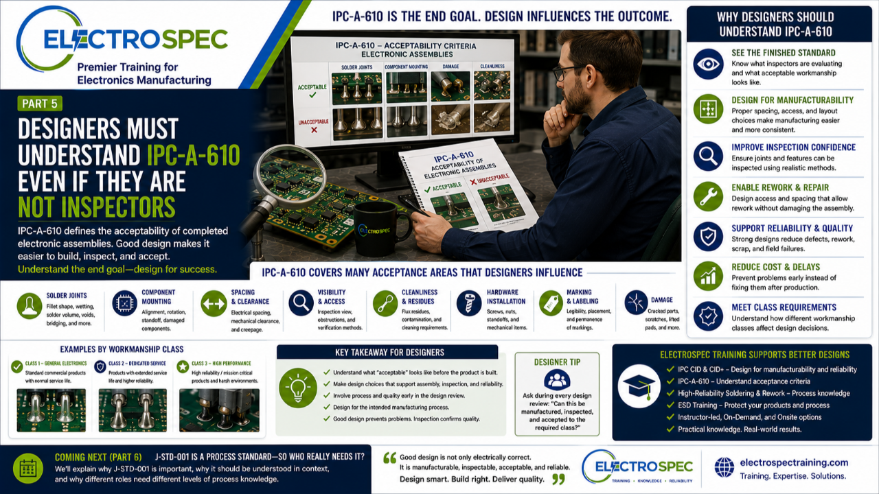
IPC-A-610 is often thought of as an inspection standard.
That is understandable.
It is commonly used by inspectors, quality personnel, manufacturing teams, auditors, and customers to evaluate the acceptability of completed electronic assemblies.
But IPC-A-610 should not only matter after the product is built.
It should matter before the product is released to manufacturing.
Designers may not be responsible for final inspection, but their design decisions strongly influence whether the finished assembly can meet IPC-A-610 acceptance criteria.
A designer does not need to become an inspector.
But a designer should understand what the inspector will eventually be asked to accept or reject.
Acceptance Criteria Are the End Goal
Every manufacturing process is trying to produce an acceptable product.
For electronic assemblies, IPC-A-610 is often used to define what acceptable workmanship looks like.
That may include criteria related to:
- component mounting
- solder joints
- lead protrusion
- component alignment
- spacing
- cleanliness
- marking
- hardware installation
- damage
- conformal coating
- wire and terminal conditions
- connector installation
- printed circuit assembly workmanship
Inspectors evaluate the final condition.
But designers influence whether that final condition is realistically achievable.
Design Decisions Shape Inspection Outcomes
An inspector may find a defect at final inspection, but the cause may have started much earlier.
A marginal solder joint may be connected to pad geometry.
A difficult-to-inspect condition may be connected to component spacing.
A rework problem may be connected to access.
A repeated alignment issue may be connected to land pattern design.
A cleaning issue may be connected to component standoff, spacing, or trapped residues.
A Class 3 concern may be connected to a design that barely supports the intended manufacturing process.
These are not only production issues.
They are design issues.
Designers Influence Solder Joint Acceptability
Solder joint acceptability is not determined only by the soldering process.
Designers influence solder joint formation through:
- land pattern design
- pad size
- pad spacing
- component package selection
- lead or termination geometry
- solder mask design
- thermal relief
- copper balance
- board finish
- component finish
- component orientation
- spacing for solder access
- inspection visibility
For SMT assemblies, the final solder joint is strongly affected by solder paste volume, stencil design, placement accuracy, and reflow profile.
For through-hole assemblies, it may be affected by hole size, lead diameter, board thickness, thermal mass, and soldering method.
IPC-A-610 may be used to inspect the finished joint, but design decisions often determine whether that joint can be formed consistently.
Component Spacing Affects Acceptability
Dense layouts may save board space, but they can create inspection and manufacturing problems.
When components are too close together, it may become difficult to:
- inspect solder joints
- verify component alignment
- clean residues
- perform rework
- use tooling
- prevent bridging
- avoid mechanical interference
- verify polarity or orientation
- maintain required spacing
The product may look efficient in CAD, but manufacturing may struggle to build and inspect it.
Designers should consider whether the final assembly can be accepted using realistic inspection methods.
Hidden Joints Require a Verification Strategy
Many modern components have solder joints that cannot be fully inspected visually.
Examples may include:
- BGAs
- bottom termination components
- certain leadless packages
- hidden gull-wing terminations
- shielded assemblies
- dense connector areas
- stacked or obstructed components
If a solder joint cannot be visually inspected, the organization must decide how it will be verified.
That may involve:
- X-ray inspection
- automated optical inspection
- electrical test
- process validation
- first article inspection
- design controls
- supplier controls
- process monitoring
Designers should not wait until inspection to discover that a feature cannot be verified.
Design for inspection begins during layout.
Class 3 Designs Need Extra Attention
Class 3 products are often associated with high-performance or high-reliability applications.
These may include aerospace, defense, medical, transportation, infrastructure, or mission-critical products where continued performance matters.
When Class 3 acceptance criteria apply, designers should be especially aware of how layout decisions affect manufacturability and inspection.
Class 3 designs should avoid relying on marginal conditions that barely pass inspection.
The goal should be robust manufacturability and reliable performance, not just minimum compliance.
A design that routinely produces borderline workmanship is not a strong design.
Inspection Is Not a Design Fix
Inspection can identify nonconforming product.
It cannot redesign the board.
It cannot move components farther apart.
It cannot change land patterns.
It cannot add missing access.
It cannot correct poor thermal relief.
It cannot change package selection.
It cannot make a hidden joint visible.
By the time inspection discovers the problem, the organization may already be dealing with rework, scrap, delays, customer questions, or qualification risk.
Designers who understand acceptance criteria can prevent many of those issues before the first board is built.
IPC-A-610 Helps Designers See the Finished Product
IPC-A-610 gives designers a practical view of what happens after release.
It helps designers understand:
- what inspectors evaluate
- what finished solder joints should look like
- what assembly conditions may be unacceptable
- how component mounting affects acceptability
- how damage is evaluated
- how spacing and alignment matter
- how workmanship criteria differ by class
- how design decisions affect inspection confidence
This knowledge makes designers better at preventing manufacturing and acceptance problems.
Designers Still Need Design-Focused Training
Understanding IPC-A-610 does not replace design training.
Designers still need deeper knowledge of PCB design principles, fabrication requirements, material selection, manufacturability, reliability, and layout practices.
That is where IPC CID and CID+ become important.
IPC-A-610 shows what the completed assembly must look like.
CID and CID+ help designers understand how to create designs that can be fabricated, assembled, inspected, and relied upon.
The two perspectives support each other.
A Better Design Review Question
Instead of asking only:
“Does this design meet the electrical requirements?”
design teams should also ask:
“Can this design be manufactured and accepted to the required workmanship class?”
That question brings IPC-A-610 into the design review process where it belongs.
It helps identify risks before production begins.
Final Thought
IPC-A-610 is not only useful after the product is built.
It is also valuable before the product is released.
Designers do not need to become inspectors, but they should understand the acceptance criteria their products must eventually meet.
A good design is not only electrically correct.
It is manufacturable, inspectable, acceptable, and reliable.
When designers understand IPC-A-610, they make better decisions that support manufacturing success, inspection confidence, and long-term product reliability.
Related ElectroSpec Training
ElectroSpec’s IPC CID and CID+ training programs help PCB designers and product engineers understand how design decisions affect fabrication, assembly, inspection, acceptance, and reliability.
ElectroSpec also offers IPC-A-610 certification for personnel who need a deeper understanding of completed electronic assembly acceptance criteria.
Coming Next
J-STD-001 Is a Process Standard—So Who Really Needs It?
In the next article, we will explain why J-STD-001 is important, why it should be understood in context, and why different roles need different levels of soldering process knowledge.