HDI and Advanced PCB Design: More Than Dense Routing
Aug 09, 2026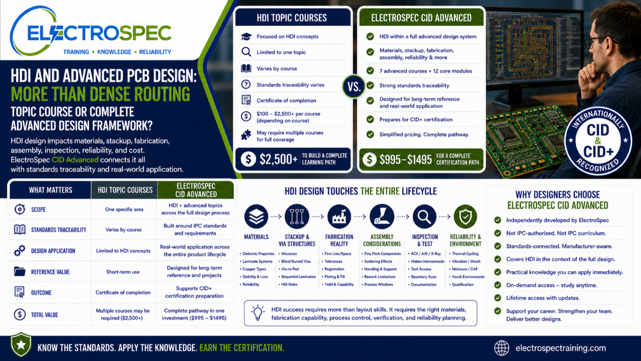
HDI design is often described as advanced PCB design.
That is true.
But HDI is not simply dense routing.
It is not just smaller traces, smaller vias, finer pitch components, and more compact geometry.
HDI changes the design problem.
It affects materials, stackup, via structures, fabrication capability, assembly yield, inspection strategy, reliability, cost, documentation, and qualification risk.
That is why HDI and advanced PCB design training matters.
But when comparing training options, designers and employers should ask an important question:
Is HDI being taught as a standalone topic, or is it part of a broader advanced design framework tied to materials, fabrication, reliability, standards traceability, and CID+ certification preparation?
That distinction matters.
A topic course may introduce advanced design concepts.
A standards-based advanced pathway helps the designer understand how those concepts connect to real products.
HDI Is Not Just Smaller Geometry
HDI design often involves:
- fine lines and spaces
- microvias
- blind vias
- buried vias
- via-in-pad
- sequential lamination
- high-density component packaging
- fine-pitch BGAs
- controlled impedance
- reduced routing channels
- tighter fabrication tolerances
- advanced materials
- higher layer counts
- signal integrity concerns
- thermal management
- higher inspection complexity
- greater reliability sensitivity
That is why HDI requires more than layout skill.
The designer must understand what the fabricator can build, what the assembly process can handle, how the board will be inspected, and how the product will survive real-world use.
A dense design that cannot be fabricated reliably is not a good design.
A compact layout that creates microvia reliability risk is not a good design.
A high-performance board that cannot be inspected or tested is not a complete design.
The Topic Course Approach
Based on the catalog examples reviewed, advanced PCB design topics may be offered as individual courses focused on advanced design concepts, emerging technologies, high-density systems, or complex PCB constraints.
Those courses can be useful.
A designer may need focused exposure to dense layout, advanced packaging, design constraints, or emerging PCB technologies.
That type of course can help fill a knowledge gap.
But HDI and advanced design do not exist in isolation.
A designer who studies only dense routing may still need to understand:
- fabrication limitations
- material selection
- stackup construction
- via reliability
- lamination cycles
- copper plating
- thermal stress
- solder joint formation
- inspection access
- test access
- supplier capability
- Class 3 implications
- customer flow-downs
- qualification expectations
That is why HDI should be taught as part of a larger advanced design framework.
ElectroSpec CID Advanced Places HDI in the Full Design System
ElectroSpec’s CID Advanced training includes a dedicated HDI PCB Design Course as part of a broader advanced PCB design pathway.
The full advanced track includes:
- PCB Fabrication & Assembly
- PCB Materials
- Rigid PCB Design
- Flexible PCB Design
- HDI PCB Design
- RF/Microwave PCB Design
- Environmental Stress Screening
This matters because HDI depends on all of those areas.
HDI depends on fabrication.
HDI depends on materials.
HDI depends on stackup.
HDI depends on assembly.
HDI depends on inspection and test planning.
HDI depends on reliability expectations.
HDI depends on the intended operating environment.
A designer cannot treat HDI as only a routing strategy.
It is a system-level design decision.
Standards Traceability Matters
Advanced PCB design should not be taught only as tips or layout techniques.
Designers need traceability back to standards, requirements, and technical constraints.
A designer should be able to ask:
- Is this a generic printed board design requirement?
- Is this tied to rigid board design requirements?
- Is this tied to customer-specific HDI requirements?
- Is this tied to fabricator capability?
- Is this tied to material selection?
- Is this tied to microvia reliability?
- Is this tied to Class 3 performance expectations?
- Is this tied to assembly or soldering requirements?
- Is this tied to inspection, test, or qualification?
- Is this tied to the product environment?
- Is this a hard requirement, supplier recommendation, or engineering judgment?
That traceability matters.
Without traceability, advanced design training can become a collection of rules without context.
With traceability, the designer understands where the requirement comes from, why it exists, and how it affects the final product.
HDI Is a Fabrication Capability Problem
HDI design is highly dependent on fabrication capability.
A layout may look correct in CAD, but that does not mean it can be built reliably or repeatedly.
Designers must consider:
- minimum line width
- minimum spacing
- laser-drilled microvias
- via aspect ratio
- via stacking
- via staggering
- via filling
- via-in-pad plating
- sequential lamination
- registration tolerance
- plating uniformity
- dielectric thickness
- copper thickness
- yield loss
- supplier process capability
- inspection and test capability
These are not minor details.
They influence whether the product can be manufactured consistently.
A designer who does not understand fabrication may unintentionally create cost, schedule, quality, or reliability problems before the board is ever built.
That is why ElectroSpec CID Advanced includes both HDI design and PCB Fabrication & Assembly.
HDI Is a Materials Problem
Materials are also central to HDI design.
As density increases, material behavior becomes more important.
Designers must understand how material choices affect:
- lamination performance
- dielectric thickness control
- thermal expansion
- dimensional stability
- resin flow
- copper adhesion
- via reliability
- impedance control
- moisture absorption
- thermal cycling
- CAF resistance
- soldering performance
- long-term reliability
HDI designs often push the limits of geometry and construction.
That means material selection must be intentional.
A designer cannot separate HDI from material knowledge.
That is why ElectroSpec CID Advanced includes a dedicated PCB Materials course as part of the advanced pathway.
HDI Is a Reliability Problem
HDI reliability is not automatic.
Advanced board structures can create advanced failure modes.
Designers must think about:
- microvia reliability
- stacked microvia risk
- thermal cycling fatigue
- plating integrity
- interconnect stress
- CTE mismatch
- solder joint reliability
- board flexure
- assembly thermal exposure
- rework limitations
- harsh environment exposure
- qualification requirements
This becomes especially important for aerospace, defense, medical, industrial, automotive, and other high-reliability applications.
Dense designs may save space.
But high density must not come at the expense of long-term reliability.
HDI Is an Assembly and Inspection Problem
HDI designs often use smaller components, tighter spacing, hidden interconnects, and dense routing.
That can create assembly and inspection challenges.
Designers should consider:
- solder paste printing
- stencil design
- fine-pitch placement
- BGA and bottom termination components
- via-in-pad effects
- solder joint inspection
- X-ray inspection needs
- rework feasibility
- cleaning access
- coating access
- test point availability
- boundary scan or alternate test methods
- documentation clarity
If the design cannot be assembled, inspected, or tested with confidence, the density of the layout becomes a liability.
A strong HDI designer thinks about verification before release.
Advanced Design Requires Supplier Communication
HDI designs often require early supplier involvement.
Designers should not wait until release to find out whether the fabricator can build the structure.
Important questions include:
- Can the supplier build the proposed stackup?
- What microvia structures are preferred?
- What via structures should be avoided?
- What material systems are available?
- What tolerances are realistic?
- What yield risks exist?
- What inspection and test methods will be used?
- What documentation does the supplier need?
- What cost drivers should the designer understand?
- What reliability risks should be reviewed early?
This is not about giving up design control.
It is about designing with manufacturing reality in mind.
Courses Come and Go, But HDI Requirements Remain
Training catalogs change.
Course titles change.
Advanced design courses may be renamed, repackaged, expanded, or removed.
That is normal.
But HDI design problems do not disappear.
Designers still need a durable reference framework tied to standards, materials, supplier capability, manufacturing constraints, customer requirements, and reliability expectations.
When an HDI board has fabrication issues, assembly problems, validation failures, or field reliability concerns, the designer needs to understand the design basis.
That requires more than remembering a course title.
It requires traceability.
Certificate of Completion vs. CID+ Preparation
An HDI or advanced design topic course may provide a certificate of completion.
That can show that a student completed the course.
But a certificate of completion is not the same as a training pathway designed to support recognized PCB design certification.
ElectroSpec CID Advanced is built to support preparation for CID+ certification.
That changes the purpose of the training.
The goal is not only to introduce advanced design concepts.
The goal is to help designers connect HDI, fabrication, materials, assembly, reliability, standards traceability, and professional certification preparation.
Price and Value
Price should be compared to scope and outcome.
A single HDI or advanced design topic course may be useful for narrow exposure.
But if a designer also needs materials, fabrication, rigid board design, flex, RF, environmental reliability, assembly considerations, and certification preparation, then multiple topic courses may be needed.
That can become expensive quickly.
ElectroSpec’s simplified comparison is different.
ElectroSpec CID Advanced is commonly positioned in the $995 to $1,495 range, depending on the offering.
A broader pathway built from multiple individual topic courses can reach $2,500+ when a student needs complete coverage across advanced design areas.
The better question is:
Is the student buying one advanced design topic, or building a standards-based pathway toward CID+ certification?
Comparison Summary
| Question | HDI or Advanced Topic Course | ElectroSpec CID Advanced |
|---|---|---|
| Main purpose | Teach selected advanced PCB design concepts | Place HDI inside a broader advanced design framework |
| Scope | Course dependent | Materials, fabrication, rigid, flex, HDI, RF/microwave, ESS, reliability |
| Standards traceability | Varies by course | Built around standards and requirements |
| Reference value | May be limited to one topic | Designed for long-term reference and application |
| Manufacturing connection | Course dependent | Connects HDI to fabrication, assembly, inspection, and supplier capability |
| Outcome | Often certificate of completion | Supports CID+ certification preparation |
| Best fit | Narrow HDI or advanced exposure | Designers seeking advanced standards-based certification preparation |
HDI Designers Need an Integrated View
A strong HDI designer should ask:
- Why does this design need HDI?
- What density problem is HDI solving?
- Can the fabricator build this stackup reliably?
- Are the via structures appropriate?
- Are microvias stacked or staggered?
- What material system is required?
- What thermal stresses will the board experience?
- Can the board be assembled consistently?
- Can hidden joints and interconnects be inspected?
- Can the product be tested?
- Does the design support Class 3 or high-reliability needs?
- What qualification environment applies?
- Can the customer rely on the product in real use?
These questions show why HDI belongs inside a complete advanced design pathway.
Independently Developed by ElectroSpec
ElectroSpec’s CID Advanced courses are independently developed by ElectroSpec.
They are not IPC-authorized training and they are not official IPC curriculum.
ElectroSpec built these courses to provide practical, standards-connected, manufacturing-aware training for designers pursuing CID+ certification preparation.
The focus is not only on learning advanced topics.
The focus is on applying advanced design knowledge to real products.
Final Thought
HDI design is not simply dense routing.
It is a fabrication problem.
It is a materials problem.
It is a reliability problem.
It is an assembly and inspection problem.
It is a standards traceability problem.
A topic course may introduce HDI concepts.
ElectroSpec CID Advanced helps place HDI inside a broader standards-based framework that supports real-world design decisions and CID+ certification preparation.
HDI is not successful because it is compact.
It is successful when the designer understands how density, materials, fabrication, assembly, inspection, test, and reliability work together.
Related ElectroSpec Training
ElectroSpec’s CID Advanced training includes HDI PCB Design as part of a broader advanced PCB design pathway.
The advanced track includes PCB Fabrication & Assembly, PCB Materials, Rigid PCB Design, Flexible PCB Design, HDI PCB Design, RF/Microwave PCB Design, and Environmental Stress Screening.
Together, these courses help designers prepare for advanced design work and CID+ certification.
Coming Next
Military, Aerospace, and Extreme Environments: Buzzwords or Requirements?
In the next article, we will compare military, aerospace, and extreme environment course language with ElectroSpec’s standards-based reliability approach and explain why market labels are not the same as real design requirements.
IPC CID Certification — ElectroSpec
IPC CID+ Certification — ElectroSpec
IPC CID/CID+ Bundle — Complete PCB Design Certification — ElectroSpec