HDI PCB Design: Density, Microvias, and Fabrication Risk
Sep 17, 2026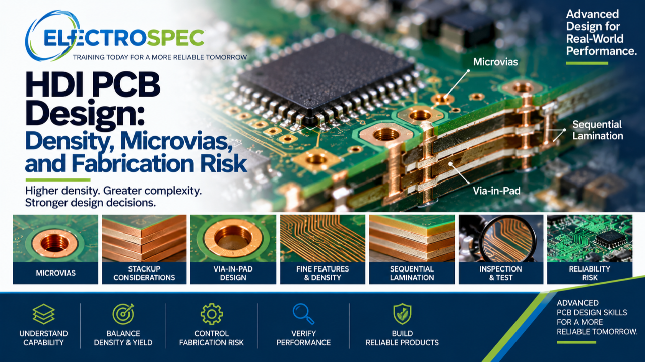
HDI design is often described as high-density routing.
That is only part of the story.
HDI design changes the way the board is fabricated, inspected, assembled, tested, and qualified. It can involve microvias, blind vias, buried vias, via-in-pad, sequential lamination, fine lines and spaces, dense component packaging, thin dielectrics, tight registration, and advanced supplier capability.
HDI can solve routing and packaging problems.
It can also create fabrication and reliability risk if it is not understood.
That is why HDI belongs in advanced PCB design training.
HDI Is a System-Level Design Decision
HDI should not be used only because it looks modern or compact.
The designer should understand why HDI is needed.
- Is the design constrained by component pitch?
- Is routing density too high for conventional vias?
- Is the product size limited?
- Is signal integrity driving layer transitions?
- Is the product high-reliability?
- Is the supplier capable of the structure?
HDI is not just a layout decision. It is a design, fabrication, supplier, inspection, and reliability decision.
Microvias Require Careful Judgment
Microvias are central to many HDI designs.
They help connect dense layers and support fine-pitch components, but they are also fabricated structures with process limits.
Designers should consider:
- microvia size
- microvia depth
- aspect ratio
- stacked versus staggered structures
- plating reliability
- via fill
- pad design
- layer transitions
- thermal cycling
- inspection and test methods
- supplier capability
A microvia is not just a small via. It is a reliability feature that must be designed and fabricated correctly.
Via-in-Pad Can Help and Hurt
Via-in-pad can be useful for dense components, thermal transfer, and routing escape.
But it must be controlled carefully.
Poor via-in-pad design can create soldering problems, voiding, insufficient solder volume, fabrication complexity, inspection challenges, and reliability risk.
Designers should understand when via-in-pad is necessary, how it will be filled or capped, how it affects assembly, and how the supplier will verify the structure.
Sequential Lamination Increases Complexity
Many HDI boards require sequential lamination.
Each lamination cycle adds cost, time, process exposure, registration challenges, material stress, and potential reliability concerns.
Designers should ask:
- How many lamination cycles are required?
- Are microvias stacked or staggered?
- What material system is being used?
- Can the supplier build the construction repeatedly?
- What inspection and test evidence will be provided?
Complex construction must be justified by product need.
Fine Features Affect Yield
HDI often uses finer lines, spaces, pads, and clearances.
Finer features can improve density, but they may also reduce process margin.
Designers should balance density against yield, cost, inspection, solder mask registration, copper thickness, etching tolerance, and supplier capability.
The smallest possible feature is not always the best design choice.
The best design choice is the one that meets requirements with acceptable manufacturing and reliability risk.
HDI Must Support Assembly
HDI design affects assembly.
Dense layouts may involve fine-pitch components, BGAs, bottom termination components, via-in-pad features, tight spacing, limited access, and hidden solder joints.
Designers should consider solder paste printing, placement, reflow, X-ray inspection, cleaning, coating, rework, and test access.
A dense board that cannot be assembled or inspected confidently creates risk.
HDI Must Support Reliability
HDI reliability is affected by materials, copper, plating, vias, thermal cycling, component packaging, assembly exposure, and environmental stress.
Designers should consider:
- thermal cycling
- CTE mismatch
- microvia fatigue
- plated interconnect reliability
- component package stress
- board flexure
- moisture exposure
- qualification requirements
- Class 3 expectations
- customer flow-downs
HDI density must not come at the expense of reliability.
Supplier Capability Is Critical
HDI requires early supplier communication.
Not every fabricator can build every HDI construction with equal confidence.
Designers should review supplier capability before release, including microvia capability, via filling, lamination cycles, minimum features, registration tolerance, material availability, controlled impedance capability, inspection methods, and reliability history.
Supplier input does not replace design requirements, but it helps determine whether the design can be built consistently.
Documentation Must Be Clear
HDI release packages must communicate the construction clearly.
Documentation may need to define stackup, materials, via structures, microvia requirements, via fill or cap requirements, controlled impedance, tolerances, inspection requirements, test requirements, qualification expectations, and objective evidence.
Ambiguity in HDI documentation can become expensive quickly.
CID Advanced Builds HDI Judgment
ElectroSpec’s CID Advanced track includes HDI PCB Design because advanced designers need to understand density, fabrication, microvias, supplier capability, reliability, and verification.
HDI is part of a larger advanced pathway that includes PCB Fabrication & Assembly, PCB Materials, Rigid PCB Design, Flexible PCB Design, RF/Microwave PCB Design, and Environmental Stress Screening.
HDI does not stand alone. It connects to the entire advanced design system.
Final Thought
HDI is not just smaller geometry.
It is a different design and fabrication problem.
Microvias, via-in-pad, sequential lamination, fine features, materials, assembly, inspection, test, supplier capability, and reliability all matter.
A strong HDI designer understands that density is only valuable when the product can still be built, verified, and trusted.
Related ElectroSpec Training
ElectroSpec’s CID Advanced training includes HDI PCB Design as part of a specialized advanced PCB design pathway.
The CID Advanced track also includes PCB Fabrication & Assembly, PCB Materials, Rigid PCB Design, Flexible PCB Design, RF/Microwave PCB Design, and Environmental Stress Screening.
Together, these courses help designers build the advanced standards-connected foundation needed for CID+ certification preparation and real-world design decisions.
Coming Next
Component Technologies and Why Package Selection Matters
In the next article, we will return to the CID Fundamentals track and discuss why component package selection affects layout, soldering, inspection, test, thermal performance, reliability, and manufacturing success.