Interconnections: Vias, Pads, Lands, Holes, and Reliability
Sep 20, 2026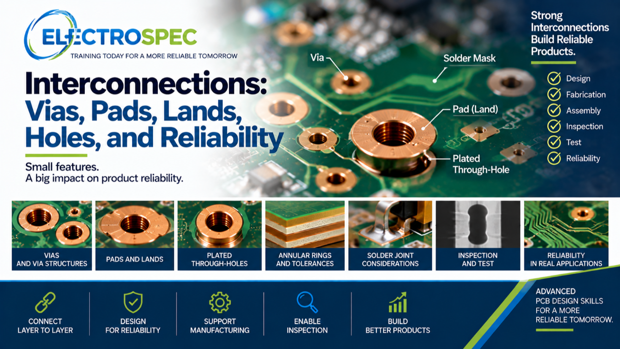
PCB interconnections may look small, but they carry the product.
Vias, pads, lands, plated through-holes, annular rings, conductors, and solderable features connect the circuit physically and electrically.
If interconnections are weak, the product is weak.
That is why PCB designers must understand interconnections as more than layout geometry.
They are fabricated structures, soldering interfaces, inspection features, and reliability elements.
Interconnections Are Physical Structures
In CAD, a via or pad may look like a simple shape.
In the real product, it becomes copper, plating, laminate, solder mask, surface finish, solder, component termination, and sometimes mechanical load.
Designers should understand that interconnections are built through fabrication and completed through assembly.
They are not just graphics on the screen.
Vias Affect Fabrication and Reliability
Vias connect layers, but they also introduce fabrication and reliability considerations.
Designers should consider via size, drill size, pad size, aspect ratio, plating thickness, annular ring, spacing, current carrying needs, thermal effects, signal behavior, supplier capability, and product class.
A via may be simple in concept, but it must be fabricated reliably.
For high-reliability products, via decisions matter.
Plated Through-Holes Carry Risk
Plated through-holes are important interconnect structures.
They may connect layers, accept component leads, support solder joints, and experience thermal and mechanical stress.
Designers should consider finished hole size, drill tolerance, lead-to-hole fit, board thickness, plating reliability, annular ring, solder fill, inspection, and thermal cycling.
A plated through-hole is not just a hole. It is a reliability feature.
Pads and Lands Shape Solder Joints
Pads and lands help define solder joint formation.
Their size, shape, spacing, mask definition, thermal connection, surface finish, and location affect solderability, placement, solder volume, inspection, and rework.
A poor land pattern can make good soldering difficult.
The component may be correct, but the solder joint may still suffer because the land pattern does not support the process.
Annular Ring Matters
Annular ring supports registration, drilling tolerance, plating reliability, and fabrication acceptance.
Designers should understand how annular ring is affected by pad size, drill size, finished hole diameter, layer registration, supplier capability, and product class.
Small annular ring decisions can affect large reliability concerns.
Interconnections Affect Inspection
Designers should think about whether interconnections can be inspected.
- Can solder joints be viewed?
- Are hidden joints addressed?
- Is X-ray needed?
- Can plated holes be verified?
- Can test points be accessed?
- Can coating or cleanliness be inspected?
A design that prevents verification creates acceptance risk.
Interconnections Affect Testability
Interconnections also affect test access.
Test points, vias, pads, connectors, and exposed copper features may support programming, in-circuit test, functional test, boundary scan, troubleshooting, and qualification monitoring.
Designers should plan test access before release.
A circuit that cannot be tested confidently is difficult to accept confidently.
Interconnections Affect Reliability in the Field
Interconnections may experience thermal cycling, vibration, shock, board flexure, current loading, humidity, contamination, and handling stress.
Designers should consider how interconnect structures will survive real use.
This is especially important for Class 3, aerospace, defense, medical, industrial, and harsh-environment products.
Reliability begins with the physical connections.
Documentation Must Communicate Interconnect Requirements
Release packages should clearly communicate hole sizes, finished hole requirements, plating requirements, via structures, pad requirements, controlled impedance features, solder mask, surface finish, inspection requirements, and test requirements.
Manufacturing cannot protect requirements that are not communicated.
CID Builds Interconnection Awareness
ElectroSpec’s CID Fundamentals course includes interconnections because PCB designers need to understand how vias, pads, lands, holes, and conductors become real product features.
The course provides 22+ hours of self-paced, on-demand PCB design training across 12 structured modules covering materials, layout principles, mechanical and electrical considerations, thermal management, component technologies, interconnections, fabrication requirements, documentation, quality assurance, manufacturability, and standards-based design thinking.
Final Thought
Interconnections are not small details.
They are the physical network that makes the product work.
Vias, pads, lands, plated through-holes, annular rings, and solderable features affect fabrication, assembly, inspection, test, reliability, and product performance.
A strong PCB designer understands that every connection must be buildable, verifiable, and reliable.
Related ElectroSpec Training
ElectroSpec’s CID Fundamentals course provides 22+ hours of self-paced, on-demand PCB design training across 12 structured modules.
The course helps designers build a standards-connected foundation in materials, layout, mechanical and electrical considerations, component technologies, interconnections, fabrication, documentation, quality, and design decision-making while preparing for CID certification.
Coming Next
Environmental Stress Screening: Designing for the Real World
In the next article, we will return to the CID Advanced track and discuss why ESS and harsh-environment thinking help designers understand how shock, vibration, thermal cycling, humidity, and qualification affect real products.