
IPC CID Certification: The Missing Link Between PCB Design, Fabrication & Assembly
Jun 17, 2026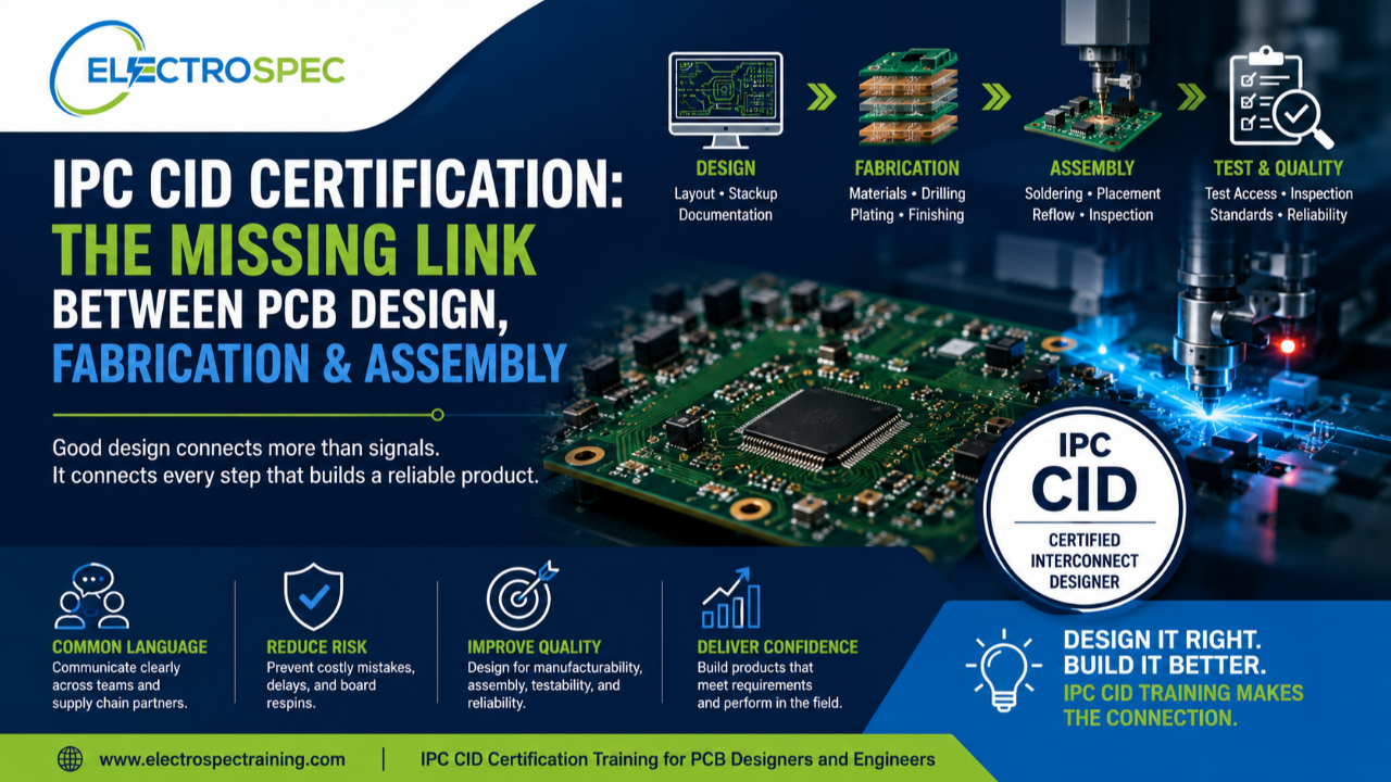
IPC CID Certification: The Missing Link Between PCB Design, Fabrication & Assembly
PCB design does not end when the layout is complete.
A board may look good on the screen, pass basic design rule checks, and still create problems when it reaches fabrication, assembly, inspection, test, or field use.
That is why IPC CID certification matters.
IPC CID, Certified Interconnect Designer, helps PCB designers and engineers understand the full connection between design intent, fabrication capability, assembly requirements, inspection expectations, and product reliability.
In many organizations, design, fabrication, and assembly operate like separate worlds. The designer creates the layout. The fabricator builds the bare board. The assembler places and solders the components. Quality inspects the finished assembly. Test verifies function.
But the product does not experience those steps separately.
The product experiences them as one continuous manufacturing chain.
CID training helps designers understand that chain.
Design Intent Is Only the Beginning
Every PCB starts with intent.
The schematic defines electrical function. The layout defines physical implementation. The documentation tells suppliers what to build.
But design intent alone is not enough.
A design must be translated into something that can be fabricated, assembled, inspected, tested, and supported.
That translation is where many problems begin.
A designer may intend for a board to be compact, high-density, high-speed, low-cost, and easy to build. But if fabrication tolerances, assembly spacing, material requirements, test access, or documentation are not considered, the final product may not meet that intent.
CID training helps designers move beyond “the board is routed” and think about whether the board is ready for manufacturing.
Fabrication Needs More Than Gerber Files
Fabricators need clear, complete, and manufacturable data.
A PCB fabrication shop must understand the board stackup, materials, copper weights, hole requirements, plating, surface finish, solder mask, controlled impedance, tolerances, markings, and acceptance requirements.
When that information is incomplete or unclear, the fabricator has to stop and ask questions.
That creates delay.
In some cases, the fabricator may make assumptions. That creates risk.
CID training helps designers understand fabrication concerns such as:
- Board materials
- Layer stackup
- Copper thickness
- Trace and space limits
- Finished hole size
- Drilled hole size
- Plating requirements
- Annular ring
- Aspect ratio
- Via structures
- Solder mask registration
- Surface finish
- Controlled impedance
- Fabrication notes
- Drawing requirements
- Supplier capability
A designer does not need to run the fabrication line, but a designer should understand how layout decisions affect fabrication success.
CID helps build that understanding.
Assembly Needs Design Choices That Support Production
A bare board can be fabricated correctly and still be difficult to assemble.
Assembly teams need land patterns, spacing, orientation markings, solderability, thermal relief, component access, rework access, cleaning access, and test access that support the actual manufacturing process.
Many assembly problems begin during layout.
For example:
- Components placed too close together can make inspection or rework difficult.
- Poor land patterns can cause solder joint defects.
- Missing polarity marks can create orientation mistakes.
- Poor thermal balance can contribute to soldering problems.
- Inadequate test access can make troubleshooting harder.
- Tight spacing can increase risk of bridging or cleaning problems.
- Poor documentation can lead to inconsistent assembly interpretation.
CID training helps designers consider design for assembly, not just design for connectivity.
The goal is not simply to place every part on the board. The goal is to place parts in a way that supports reliable assembly.
Inspection and Quality Need Clear Acceptance Criteria
Quality inspection depends on clear requirements.
Inspectors need to know product class, applicable standards, drawing requirements, workmanship expectations, and customer-specific acceptance criteria.
Designers influence many of those inspection outcomes.
If documentation does not define the correct class, finish, notes, special requirements, test points, markings, or assembly expectations, inspection becomes harder and less consistent.
CID training helps designers understand how their design package supports inspection and quality.
A strong design package helps answer:
- What class is this product built to?
- What standards apply?
- What finish is required?
- What markings are required?
- What tolerances apply?
- What inspection features are available?
- Are there special assembly or reliability concerns?
- Are fabrication and assembly requirements clear?
When design documentation is complete, quality teams can inspect more consistently, suppliers can build more confidently, and customers receive a more reliable product.
Test Access Is a Design Decision
Testing is often treated as something that happens after assembly.
But testability begins during design.
If test points are missing, inaccessible, poorly placed, or not documented, the test team may struggle to verify the product efficiently.
Poor test access can increase troubleshooting time, delay production, and make failure analysis more difficult.
CID training helps designers remember that test is part of product lifecycle.
A good PCB design considers:
- Test point access
- Probe clearance
- Fixture requirements
- Boundary scan needs
- Programming access
- Debug access
- Ground access
- Signal accessibility
- Marking and documentation
- Production test flow
A board that cannot be tested efficiently may become expensive even if it functions correctly.
Design for test is part of designing it right.
Reliability Is Built Across the Whole Chain
Reliability is not created by one department.
It is built across design, fabrication, assembly, inspection, and test.
Designers affect reliability through material choices, spacing, stackup, thermal management, component placement, hole structures, land patterns, conductor geometry, and documentation.
Fabricators affect reliability through process control, plating quality, registration, material control, and workmanship.
Assemblers affect reliability through soldering, cleaning, handling, component placement, and process control.
Inspectors and test personnel help verify that the product meets requirements.
CID training helps designers understand how their decisions fit into that larger reliability picture.
A design decision that saves space may increase assembly difficulty. A design decision that reduces fabrication cost may increase field risk. A design decision that looks simple in layout may create inspection or test problems later.
CID helps designers think through those tradeoffs before the product reaches production.
CID Creates a Common Technical Language
One of the greatest benefits of IPC CID certification is communication.
PCB design involves many groups:
- PCB designers
- Electrical engineers
- Mechanical engineers
- Fabricators
- Assembly suppliers
- Process engineers
- Manufacturing engineers
- Quality inspectors
- Test engineers
- Program managers
- Customers
Each group sees the product from a different angle.
CID training helps create a common technical language across those groups.
When designers understand IPC design principles, they can communicate more effectively with fabrication and assembly suppliers.
When engineers understand manufacturing constraints, they can make better design choices.
When quality teams understand design intent, they can ask better questions.
When suppliers receive better documentation, they can build with fewer delays and fewer assumptions.
That communication reduces friction across the supply chain.
CID Helps Prevent the “Throw It Over the Wall” Problem
One of the most common problems in electronics manufacturing is the “throw it over the wall” mindset.
Design completes the layout and sends it to fabrication.
Fabrication raises questions.
Assembly finds issues.
Inspection identifies defects.
Test finds failures.
Then everyone works backward to determine where the problem started.
CID training helps reduce that cycle.
It encourages designers to think ahead and consider how fabrication, assembly, inspection, and test will use the design.
Instead of throwing the design over the wall, CID-trained designers help build a bridge across the wall.
That is why CID is the missing link.
Better Designers Understand the Full Product Path
A strong PCB designer is not just someone who knows layout software.
A strong designer understands the product path:
- Electrical intent
- Mechanical constraints
- PCB layout
- Fabrication capability
- Assembly process
- Inspection criteria
- Test access
- Reliability expectations
- Documentation control
- Supplier communication
CID training helps designers connect these steps.
That connection makes the designer more valuable to the company because they can help prevent problems earlier in product development.
The best designers do not simply complete layouts.
They help create manufacturable, inspectable, testable, and reliable products.
Who Benefits from IPC CID Certification?
IPC CID certification is especially useful for PCB designers and layout professionals, but it also benefits many other roles.
CID is valuable for:
- PCB designers
- PCB layout professionals
- Electrical engineers
- Product engineers
- Manufacturing engineers
- Process engineers
- Quality engineers
- Design reviewers
- Engineering managers
- Technical leads
- Program teams working with PCB suppliers
Anyone involved in PCB design decisions can benefit from understanding how those decisions affect downstream manufacturing and product quality.
ElectroSpec Training’s IPC CID Course
ElectroSpec Training provides IPC CID certification preparation for PCB designers, engineers, and technical professionals who want practical, standards-based training.
Our CID course helps students understand the design concepts, IPC expectations, documentation practices, and exam topics needed to prepare for certification.
ElectroSpec’s CID training supports:
- On-demand learning
- Practical exam preparation
- Standards-based instruction
- Study support
- Practice questions
- Instructor support
Whether you are a new designer, experienced layout professional, engineer, or technical manager, CID certification can help strengthen your understanding of PCB design and manufacturing relationships.
Final Thought
PCB design, fabrication, and assembly cannot be treated as separate islands.
They are connected.
A design choice affects fabrication. Fabrication affects assembly. Assembly affects inspection. Inspection affects delivery. Test affects confidence. Reliability affects the customer.
IPC CID training helps designers understand those connections.
That is why CID certification is so valuable.
It is the missing link between design intent and manufacturing reality.
Design with fabrication in mind. Design with assembly in mind. Design with reliability in mind.
ElectroSpec Training offers IPC CID certification preparation for PCB designers, engineers, layout professionals, and technical teams who want to improve design quality and reduce manufacturing risk.
Prepare with flexible on-demand training, practical exam preparation, practice questions, and instructor support.
Connect design intent to manufacturing reality with IPC CID training.
