
IPC CID Certification: Why PCB Designers Need More Than Layout Software Skills
Jun 15, 2026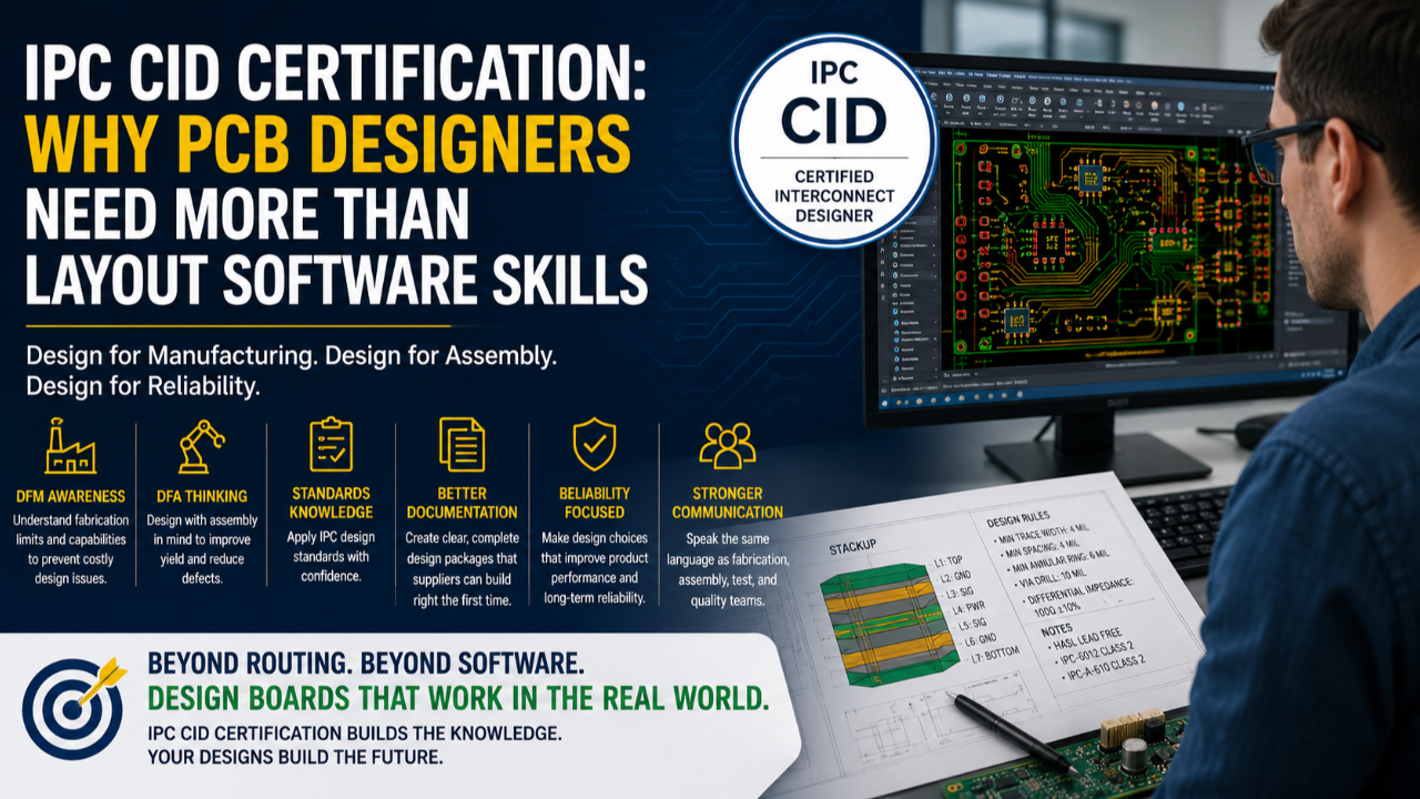
IPC CID Certification: Why PCB Designers Need More Than Layout Software Skills
Modern PCB design is more than drawing traces, placing components, and generating Gerber files.
Layout software is powerful. It can help route a board, check spacing, manage layers, create footprints, and export manufacturing data. But software alone does not make someone a strong PCB designer.
A good PCB designer must understand how the design will be fabricated, assembled, inspected, tested, and supported in the real world.
That is where IPC CID certification becomes valuable.
IPC CID, Certified Interconnect Designer, helps bridge the gap between knowing how to use PCB layout tools and understanding how to design printed boards that can actually be built reliably.
Layout Software Is Only the Tool
PCB layout software is like a drafting table with intelligence built in. It helps the designer create the board, but it does not replace engineering judgment.
A design tool may allow a trace width, via structure, pad size, spacing, or layer stackup that is technically possible inside the software but difficult, expensive, or risky to manufacture.
The software may not fully understand:
- Fabrication limits
- Assembly process risks
- Material selection
- Plating requirements
- Hole-to-pad relationships
- Annular ring concerns
- Solder joint reliability
- Component land pattern issues
- Impedance control tradeoffs
- Documentation requirements
- Inspection and test access
- Supplier capability
That is why a PCB designer needs more than tool knowledge.
The designer must understand the relationship between design choices and manufacturing outcomes.
CID Training Connects Design to Manufacturing Reality
IPC CID training helps designers think beyond the screen.
The course focuses on standards, design rules, documentation practices, and manufacturing considerations that support reliable printed board design.
A strong designer understands that every layout decision has consequences.
A small annular ring may create fabrication yield problems. Poor component spacing may create assembly access issues. Incorrect land patterns may cause solder joint defects. Weak documentation may delay fabrication. Poor stackup planning may create signal integrity, impedance, or reliability concerns. Missing notes or unclear requirements may create supplier confusion.
CID training helps designers understand how those problems begin at design stage and how to prevent them before the board ever goes out for fabrication.
Why CID Matters for PCB Designers
A PCB designer is often the person who turns engineering intent into a manufacturable product.
That means the designer must understand more than schematic connectivity.
The designer must consider:
- Can the board be fabricated?
- Can the board be assembled?
- Can the board be inspected?
- Can the board be tested?
- Can the board survive the intended environment?
- Can the supplier understand the documentation?
- Can the design be produced repeatedly without unnecessary cost or risk?
CID certification gives designers a stronger foundation in these areas.
It helps designers speak the same language as fabrication shops, assembly houses, product engineers, process engineers, and quality teams.
That common language is important because many PCB problems are not caused by bad intent. They are caused by gaps between design, fabrication, assembly, and inspection.
CID helps close those gaps.
The Cost of Design Mistakes
PCB design mistakes can be expensive.
A small design issue can lead to:
- Fabrication delays
- Supplier questions
- Engineering change requests
- Board respins
- Assembly defects
- Soldering problems
- Test failures
- Reliability concerns
- Schedule slips
- Increased cost
The worst time to find a design issue is after boards are built.
By then, the cost is higher, schedule pressure is greater, and options are limited.
CID training helps designers identify risk earlier, when changes are easier and less expensive.
That is one of the biggest values of IPC CID certification: it improves design decision-making before manufacturing begins.
CID Is Valuable for More Than PCB Layout Designers
IPC CID is especially valuable for PCB designers and layout professionals, but it is also useful for many other roles.
Electrical engineers benefit because they gain a better understanding of how design requirements translate into physical board construction.
Manufacturing engineers benefit because they can better communicate design-for-manufacturing concerns.
Quality engineers benefit because they understand how design decisions affect inspection, acceptance, and reliability.
Program managers benefit because they better understand why design rules, supplier capability, and documentation quality affect cost and schedule.
CID is not only about drawing boards. It is about understanding the full printed board design process.
Better Design Documentation Means Fewer Problems
One of the most overlooked parts of PCB design is documentation.
A board is not complete just because the layout is finished.
Fabrication and assembly suppliers need clear, complete, and controlled documentation. That includes drawings, notes, material requirements, stackup information, tolerances, finishes, hole requirements, markings, and other design details.
Poor documentation creates assumptions. Assumptions create variation. Variation creates risk.
CID training reinforces the importance of design documentation so the board can be built as intended.
A good design package helps suppliers quote accurately, fabricate correctly, assemble efficiently, and reduce back-and-forth engineering questions.
CID Helps Designers Communicate Across the Supply Chain
PCB design sits at the intersection of multiple teams.
Designers communicate with electrical engineers, mechanical engineers, fabrication suppliers, assembly suppliers, test engineers, quality inspectors, and customers.
CID training helps create a shared technical foundation.
When designers understand IPC design principles, they can have better conversations about:
- Design rules
- Fabrication capability
- Assembly constraints
- Land patterns
- Stackups
- Materials
- Hole structures
- Spacing
- Solderability
- Inspection access
- Reliability expectations
This makes the designer more valuable because they are not just operating software. They are helping reduce risk across the product lifecycle.
Software Skills Start the Design — CID Knowledge Strengthens It
There is nothing wrong with being skilled in PCB layout software. In fact, tool proficiency is essential.
But software skill is only one part of professional PCB design.
The stronger designer combines software skill with standards knowledge, manufacturing awareness, documentation discipline, and practical design judgment.
That is the real value of IPC CID certification.
CID helps designers move from “I can route the board” to “I can design a board that can be fabricated, assembled, inspected, tested, and supported.”
That is a much higher level of capability.
Who Should Consider IPC CID Certification?
IPC CID certification is a strong fit for:
- PCB designers
- PCB layout professionals
- Electrical engineers
- Product engineers
- Manufacturing engineers
- Quality engineers
- Design team leads
- Engineering managers
- Anyone involved in printed board design reviews
It is especially valuable for professionals who want to strengthen their understanding of IPC design standards and improve the quality of their printed board design packages.
ElectroSpec Training’s IPC CID Course
ElectroSpec Training provides IPC CID certification preparation designed to help students understand the standard, prepare for the exam, and apply design knowledge in real manufacturing environments.
Our CID training is built for busy professionals who need practical, flexible, and focused preparation.
The course includes on-demand training, study support, practice questions, and exam preparation to help students build confidence before certification testing.
Whether you are new to PCB design or an experienced designer looking to strengthen your credentials, CID certification can help show that you understand more than layout software.
It demonstrates that you understand the design principles behind reliable printed boards.
Final Thought
PCB design is not just about completing a layout.
It is about creating a design that can move successfully from concept to fabrication, assembly, inspection, test, and field use.
Layout software helps create the board.
IPC CID training helps create a better designer.
For professionals who want to improve PCB design knowledge, reduce manufacturing risk, and build stronger design packages, IPC CID certification is a valuable next step.
Design it right before it reaches the shop floor.
Call to Action
ElectroSpec Training offers IPC CID certification preparation for PCB designers, engineers, and technical professionals who want practical, standards-based training.
Prepare for your CID certification with flexible on-demand training, focused exam preparation, and instructor support.
Learn the standard. Improve the design. Reduce manufacturing risk.
