PCB Fabrication and Assembly Realities for Advanced Designers
Sep 09, 2026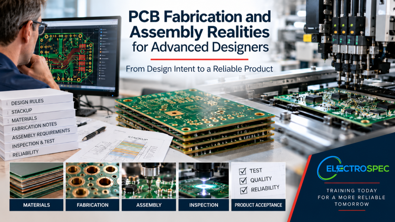
Advanced PCB design does not end at the layout screen.
A design may look clean in CAD, pass design rule checks, and meet the electrical intent, but still create problems during fabrication, assembly, inspection, test, or qualification.
That is why advanced designers must understand fabrication and assembly realities.
A PCB is not only designed.
It is built.
It is processed.
It is inspected.
It is tested.
It is accepted or rejected based on real manufacturing results.
The stronger designer understands that every layout decision eventually becomes a manufacturing condition.
Fabrication Turns the Design Into a Physical Board
Fabrication is where the design becomes a real printed board.
The fabricator must turn drawings, data files, material requirements, stackup information, hole tables, copper features, solder mask, surface finish, and tolerances into a physical product.
Advanced designers should understand how fabrication is affected by:
- laminate selection
- stackup design
- copper thickness
- conductor width and spacing
- hole size
- plated through-hole requirements
- via structures
- annular ring
- layer registration
- solder mask registration
- surface finish
- controlled impedance
- panelization
- dimensional tolerances
- supplier capability
These are not only supplier concerns.
They are design concerns.
A design that pushes fabrication limits may increase cost, reduce yield, extend lead time, or create reliability risk.
Assembly Turns the Board Into a Product
After fabrication, the board must be assembled.
Assembly brings a different set of realities.
The design must support component placement, soldering, cleaning, coating, inspection, test, and handling.
Assembly considerations include:
- SMT reflow
- through-hole assembly
- wave soldering
- selective soldering
- manual soldering
- press-fit components
- solder paste printing
- stencil design
- thermal balance
- component spacing
- connector access
- cleaning access
- conformal coating
- staking or bonding
- rework access
- inspection access
- test access
A layout that ignores assembly can create solder defects, inspection problems, test delays, rework difficulty, or product escapes.
Good design gives assembly a fair chance to succeed.
Advanced Designs Create Advanced Manufacturing Risk
The more advanced the board, the more important fabrication and assembly knowledge becomes.
A simple board may tolerate more margin.
An advanced board may not.
HDI designs may require microvias, blind vias, buried vias, via-in-pad, sequential lamination, tight registration, and careful supplier review.
RF and microwave designs may require controlled materials, tight impedance control, copper roughness awareness, clean transitions, and careful stackup control.
Flex and rigid-flex designs may require attention to bend radius, coverlay, adhesives, stiffeners, dynamic flexing, transition zones, and mechanical stress.
Class 3 and high-reliability products may require stronger materials, better process control, more inspection confidence, and objective evidence.
Advanced design increases the importance of manufacturing awareness.
Manufacturing Capability Should Influence the Design Early
A common mistake is waiting too long to involve fabrication and assembly knowledge.
The designer completes the layout.
The files are released.
Then the supplier asks questions.
By then, changes may be more expensive.
Advanced designers should think about supplier capability before release.
They should ask:
- Can the supplier build this stackup reliably?
- Are the materials available and appropriate?
- Are the line widths and spacing realistic?
- Are the via structures appropriate?
- Are aspect ratios reasonable?
- Can controlled impedance be achieved?
- Can the assembly process support the layout?
- Can solder joints be formed consistently?
- Can the product be inspected?
- Can the product be tested?
- Can the product be cleaned, coated, or reworked if needed?
These questions belong in design review, not only after release.
Soldering Is Affected by Design
Soldering problems are often discovered during assembly, but many soldering risks begin in design.
Designers influence soldering through:
- land pattern design
- pad geometry
- hole-to-lead relationship
- thermal relief
- copper balance
- component spacing
- package selection
- board thickness
- surface finish
- solder mask design
- via placement
- component orientation
- assembly process selection
The soldering operator forms the joint.
The process engineer controls the process.
But the designer helps determine whether the design supports a good soldering outcome.
This is especially important for high-reliability products where solder joint performance, inspection, and long-term reliability matter.
Inspection Access Must Be Designed
Inspection is not something to figure out after assembly.
Advanced designers should consider inspection access early.
They should ask:
- Can solder joints be viewed?
- Are polarity markings visible?
- Are reference designators useful?
- Are bottom termination components addressed?
- Is X-ray inspection required?
- Can coating be inspected?
- Can cleanliness be verified?
- Can hardware installation be confirmed?
- Can test points be reached?
- Can acceptance evidence be produced?
If inspection is difficult, the design may need an alternate verification strategy.
That strategy should be planned before release.
Test Access Must Be Designed
Testing also depends on design.
A product may need in-circuit test, functional test, programming, boundary scan, environmental test monitoring, or diagnostic access.
Advanced designers should consider:
- test point placement
- connector access
- programming access
- diagnostic access
- fixture access
- boundary scan strategy
- functional test coverage
- failure isolation
- acceptance records
- qualification test needs
A design that cannot be tested with confidence can create production delays and weak objective evidence.
Testability is not only a test engineering concern.
It is a design concern.
Documentation Communicates Manufacturing Intent
Fabrication and assembly suppliers do not build from intent.
They build from documentation.
Advanced designers must ensure the release package clearly communicates:
- stackup
- materials
- copper thickness
- surface finish
- solder mask
- controlled impedance
- hole requirements
- fabrication tolerances
- assembly requirements
- soldering requirements
- inspection requirements
- test requirements
- coating requirements
- cleaning requirements
- qualification requirements
- records and evidence requirements
A good design can fail if the documentation is unclear.
The release package is where the designer’s intent becomes manufacturing instruction.
Supplier Questions Are Signals
Supplier questions should not be treated only as interruptions.
They often reveal where the design or documentation needs improvement.
Questions may expose:
- missing requirements
- unclear notes
- material concerns
- fabrication risk
- assembly access issues
- inspection uncertainty
- test access gaps
- conflicting documentation
- supplier capability limits
A strong designer listens to supplier questions and uses them to improve the design system.
Every good question can become a better future design rule, drawing note, checklist, or design review item.
CID Advanced Connects Fabrication and Assembly to Design
ElectroSpec’s CID Advanced track includes PCB Fabrication & Assembly because advanced designers need to understand how design choices affect real manufacturing outcomes.
This course helps connect design decisions to:
- fabrication capability
- assembly process selection
- manufacturability
- soldering outcomes
- inspection access
- testability
- documentation
- reliability
- product acceptance
It is one part of the larger CID Advanced pathway, which also includes PCB Materials, Rigid PCB Design, Flexible PCB Design, HDI PCB Design, RF/Microwave PCB Design, and Environmental Stress Screening.
That matters because fabrication and assembly do not stand alone.
They connect to the full design system.
Advanced Designers Need Manufacturing-Aware Judgment
Advanced PCB design requires judgment.
A designer may need to balance:
- electrical performance and manufacturability
- density and inspection access
- material performance and supplier availability
- cost and reliability
- schedule and qualification risk
- assembly process limits and layout goals
- customer requirements and supplier capability
There is rarely one perfect answer.
There is usually a best answer for the requirement, the product, the process, and the risk.
That is why advanced designers need more than CAD skill.
They need manufacturing-aware judgment.
Practical Questions Before Release
Before releasing an advanced PCB design, ask:
- Can the board be fabricated reliably?
- Can the assembly process build it consistently?
- Are materials appropriate and available?
- Is the stackup realistic?
- Are via structures within supplier capability?
- Is soldering risk understood?
- Can the product be inspected?
- Can the product be tested?
- Are cleaning and coating requirements clear?
- Are documentation and notes complete?
- Are supplier questions resolved?
- What evidence will prove conformance?
These questions help reduce surprises before production begins.
Final Thought
Advanced PCB design is not only about advanced layout.
It is about understanding how the layout becomes a product.
Fabrication turns the design into a board.
Assembly turns the board into a functional product.
Inspection and test verify the result.
Documentation communicates the intent.
Objective evidence proves conformance.
A strong designer understands those realities before release.
That is why fabrication and assembly knowledge belongs inside advanced PCB design training.
Related ElectroSpec Training
ElectroSpec’s CID Advanced training includes PCB Fabrication & Assembly as part of a specialized advanced PCB design pathway.
The CID Advanced track also includes PCB Materials, Rigid PCB Design, Flexible PCB Design, HDI PCB Design, RF/Microwave PCB Design, and Environmental Stress Screening.
Together, these courses help designers build the advanced manufacturing-aware foundation needed for CID+ certification preparation and real-world design decisions.
Coming Next
Layout Principles: More Than Placing Parts and Routing Traces
In the next article, we will return to the CID Fundamentals track and discuss why layout principles are not just CAD skills. Layout decisions affect manufacturability, inspection, testability, reliability, and product success.
IPC CID Certification — ElectroSpec
IPC CID+ Certification — ElectroSpec
IPC CID/CID+ Bundle — Complete PCB Design Certification — ElectroSpec