From Requirement Flow-Down to PCB Layout: How Standards Become Design Decisions
Aug 25, 2026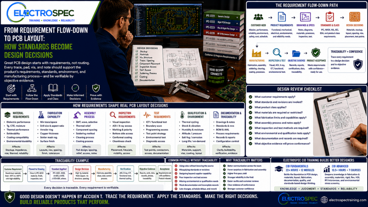
PCB layout is not the beginning of design.
It is the result of many decisions that came before it.
Before a trace is routed, before a via is placed, before a component is positioned, and before a fabrication package is released, the designer should understand the requirement flow-down.
That flow-down connects the customer need to the product requirement, the product requirement to the drawing, the drawing to the standards, the standards to the design choices, and the design choices to manufacturing, inspection, test, qualification, and objective evidence.
That is how standards become real design decisions.
A PCB layout is not just artwork.
It is a technical response to requirements.
Requirements Start Before the Board
A printed circuit board exists because a product has a purpose.
That purpose may come from a customer, system requirement, contract, product specification, mission need, or internal design objective.
Before the layout begins, the designer should understand:
- What must the product do?
- Where will it operate?
- What environment will it experience?
- What product class applies?
- What standards are invoked?
- What customer requirements are flowed down?
- What fabrication and assembly processes will be used?
- What inspection and test evidence will be required?
- What qualification expectations apply?
Without these answers, the layout may move quickly, but it may move in the wrong direction.
The Drawing Package Carries the Obligation
The drawing package is where many requirements become visible.
Drawings, notes, specifications, bills of material, approved manufacturer lists, fabrication requirements, assembly requirements, inspection notes, and test requirements help define what the product must meet.
A designer should not treat drawing notes as administrative text.
Drawing notes may define:
- product class
- standards and revisions
- material requirements
- surface finish
- solder mask
- conductor and spacing expectations
- fabrication tolerances
- assembly requirements
- cleaning requirements
- conformal coating requirements
- inspection criteria
- test requirements
- serialization or traceability requirements
- qualification requirements
The layout must support those notes.
If the drawing says one thing and the layout makes that requirement difficult or impossible, the design package is not aligned.
Product Class Affects Design Decisions
Product class is not just an inspection label.
Class expectations can influence design decisions from the beginning.
A Class 3 or high-reliability product may require stronger attention to materials, fabrication capability, solder joint reliability, inspection access, testability, documentation, process control, and objective evidence.
Designers should ask:
- Does the selected material support the product class?
- Are conductor widths and spacings appropriate?
- Are annular rings and via structures reasonable?
- Can solder joints be formed consistently?
- Can the product be inspected?
- Can the product be tested?
- Can the product be cleaned and coated if required?
- Can the design survive the intended environment?
The product class should influence the layout, not merely appear in the documentation after the design is complete.
Standards Translate Requirements Into Design Constraints
Standards help convert broad requirements into specific design considerations.
For example:
A reliability requirement may affect material selection, stackup, via structures, solder joint design, and test planning.
A fabrication requirement may affect line width, spacing, annular ring, copper thickness, solder mask, surface finish, and tolerances.
An assembly requirement may affect land patterns, thermal relief, component spacing, soldering method, cleaning access, and coating strategy.
An inspection requirement may affect component placement, visibility, marking, test access, X-ray access, and documentation.
A qualification requirement may affect materials, mechanical support, connectors, solder joints, coating, and environmental test planning.
This is where standards traceability becomes practical.
The designer must understand how requirements become constraints in the layout.
Material Requirements Shape the Layout
Material selection is not separate from layout.
The material system affects electrical performance, fabrication, soldering, thermal behavior, moisture resistance, dimensional stability, and reliability.
Material decisions may influence:
- stackup
- dielectric thickness
- impedance control
- conductor geometry
- via reliability
- thermal performance
- soldering exposure
- flexural behavior
- coating compatibility
- environmental durability
A high-speed design, RF design, flex circuit, HDI board, high-current board, or harsh-environment product may require material decisions before layout can be finalized.
A designer who chooses geometry without understanding material behavior may create hidden reliability risk.
Fabrication Capability Must Flow Into Layout
The fabricator’s capability should influence layout before release.
A design should consider:
- minimum conductor width
- minimum spacing
- copper thickness
- board thickness
- layer count
- drill size
- via aspect ratio
- annular ring
- plating capability
- solder mask registration
- surface finish
- controlled impedance capability
- HDI capability
- flex or rigid-flex capability
- panelization
- tolerances
A layout that exceeds supplier capability may still look clean in CAD.
But CAD does not prove manufacturability.
Designers should understand fabrication limits early, especially for Class 3, HDI, RF, flex, rigid-flex, and harsh-environment products.
Assembly Process Must Shape the Layout
Assembly is also part of requirement flow-down.
The layout should support the process that will actually build the product.
That may include:
- SMT reflow
- wave soldering
- selective soldering
- manual soldering
- robotic soldering
- press-fit installation
- cleaning
- conformal coating
- staking or bonding
- inspection
- test
- rework, when allowed
A layout that ignores assembly process may create solder defects, access problems, cleaning problems, coating problems, or inspection difficulty.
The solder joint is formed in manufacturing, but many solder joint risks begin in design.
Inspection Access Must Be Designed In
Inspection should not be an afterthought.
Designers should ask:
- Can solder joints be inspected?
- Are polarity marks visible?
- Are reference designators useful?
- Can bottom termination components be verified?
- Is X-ray inspection required?
- Are test points accessible?
- Can coating be inspected?
- Can cleanliness be verified?
- Can hardware installation be confirmed?
- Can defects be detected with confidence?
A layout that prevents inspection creates acceptance risk.
If a feature cannot be inspected directly, the design package should identify the alternate verification method.
Test Requirements Must Influence Layout
Testing also flows into design.
A product may require in-circuit test, functional test, boundary scan, programming, environmental monitoring, or qualification test access.
Designers should consider:
- test point placement
- connector access
- programming access
- diagnostic access
- boundary scan strategy
- functional test needs
- fixture access
- environmental test monitoring
- failure isolation
- data collection
- acceptance records
A layout that does not support test can delay production, reduce diagnostic capability, and weaken objective evidence.
Testability should be designed into the board, not negotiated after release.
Qualification Requirements Must Be Considered Early
If the product must survive shock, vibration, thermal cycling, humidity, altitude, salt fog, contamination, or other environmental stresses, those conditions should influence layout early.
Qualification requirements may affect:
- component placement
- board mounting
- connector support
- solder joint geometry
- material selection
- via structures
- coating strategy
- cleanliness
- mechanical reinforcement
- thermal paths
- inspection access
- test access
- documentation
Qualification failure is expensive because it often occurs after design, fabrication, assembly, and test money has already been spent.
Good designers consider qualification before the first layout release.
Traceability Connects Decisions to Evidence
Requirement flow-down does not end with the layout.
The design must eventually be verified.
That verification may produce objective evidence such as:
- material certifications
- fabrication records
- assembly records
- inspection reports
- test results
- qualification reports
- process control records
- configuration records
- traceability records
A traceable design decision connects the requirement to the layout, then to verification and evidence.
That is how organizations prove that the product meets requirements.
A requirement that cannot be traced may be missed.
A design decision that cannot be explained may be questioned later.
CID Builds the Requirement-to-Design Foundation
ElectroSpec’s CID Fundamentals course helps designers build the foundation needed to connect requirements to PCB design decisions.
The course includes 22+ hours of on-demand training across 12 structured modules covering materials, layout principles, mechanical and electrical considerations, thermal management, component technologies, interconnections, fabrication requirements, documentation, quality assurance, manufacturability, and standards-based design thinking.
That foundation helps designers understand how customer needs, standards, product class, materials, fabrication, assembly, inspection, and test influence layout.
CID is not only about learning PCB terminology.
It is about learning how design decisions connect to requirements.
CID Advanced Expands the Flow-Down Framework
ElectroSpec CID Advanced builds on that foundation with advanced courses in:
- PCB Fabrication & Assembly
- PCB Materials
- Rigid PCB Design
- Flexible PCB Design
- HDI PCB Design
- RF/Microwave PCB Design
- Environmental Stress Screening
These topics help designers handle more complex flow-down decisions.
A flex requirement affects bend radius, materials, coverlay, stiffeners, and mechanical support.
An HDI requirement affects microvias, sequential lamination, supplier capability, and reliability.
An RF requirement affects materials, stackup, impedance, copper, geometry, and fabrication control.
An environmental requirement affects thermal cycling, vibration, humidity, coating, solder joints, and qualification.
Advanced design requires the designer to trace requirements through the entire product lifecycle.
A Practical Flow-Down Checklist
Before releasing a PCB layout, designers should ask:
- What customer requirements apply?
- What standards and revisions are invoked?
- What product class applies?
- What materials are required or restricted?
- What fabrication capabilities and limits apply?
- What assembly process will be used?
- What soldering requirements affect the layout?
- What inspection methods are planned?
- What test access is required?
- What environmental stresses apply?
- What qualification tests are required?
- What documentation is needed?
- What objective evidence will prove conformance?
These questions help move the design from layout activity to engineering discipline.
Independently Developed by ElectroSpec
ElectroSpec’s CID and CID Advanced courses are independently developed by ElectroSpec.
They are not IPC-authorized training and they are not official IPC curriculum.
ElectroSpec developed these courses to provide practical, standards-connected, manufacturing-aware design training for students preparing for CID and CID+ certification.
The focus is not only on knowing standards.
The focus is on understanding how requirements become design decisions.
Final Thought
PCB layout is where requirements become physical.
Every trace, pad, via, material, component location, spacing decision, test point, and note should support the product’s requirement set.
Customer needs flow into drawings.
Drawings invoke standards.
Standards create constraints.
Constraints shape the layout.
Manufacturing builds the product.
Inspection and test verify the product.
Objective evidence proves conformance.
That is requirement flow-down.
A good designer does not merely route a board.
A good designer translates requirements into a product that can be built, inspected, tested, accepted, and trusted.
Related ElectroSpec Training
ElectroSpec’s CID Fundamentals course provides 22+ hours of on-demand PCB design training across 12 structured modules.
ElectroSpec’s CID Advanced training expands into PCB Fabrication & Assembly, PCB Materials, Rigid PCB Design, Flexible PCB Design, HDI PCB Design, RF/Microwave PCB Design, and Environmental Stress Screening.
Together, these courses help designers build the standards-connected foundation needed for CID and CID+ certification preparation.
Coming Next
Design Rules, Supplier Capability, and Engineering Judgment
In the next article, we will discuss why design rules are not all equal, and how designers should distinguish between standards requirements, customer requirements, supplier capability, company preferences, and engineering judgment.
IPC CID Certification — ElectroSpec
IPC CID+ Certification — ElectroSpec
IPC CID/CID+ Bundle — Complete PCB Design Certification — ElectroSpec