RF and Signal Integrity Courses: Useful Topic or Integrated Design Path?
Aug 08, 2026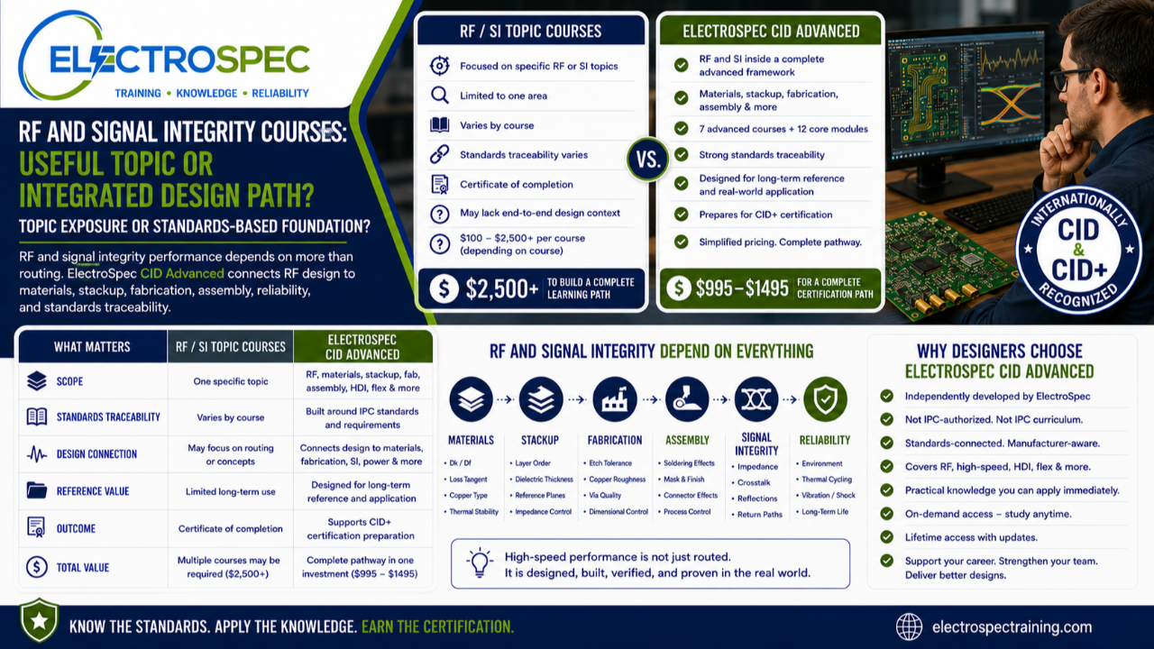
RF and signal integrity are important areas of PCB design.
As frequencies increase, rise times become faster, packaging becomes denser, and product requirements become more demanding, the PCB is no longer just a place to connect components.
The PCB becomes part of the electrical system.
That is why RF and signal integrity training matters.
But when comparing training options, designers and employers should ask an important question:
Is RF or signal integrity being taught as a standalone topic, or is it part of a broader advanced design framework tied to materials, stackup, fabrication, standards, manufacturability, reliability, and certification preparation?
That distinction matters.
A topic course may introduce RF routing or signal integrity concepts.
A standards-based advanced design pathway helps the designer understand how those concepts connect to the full product design.
RF and Signal Integrity Are Not Only Routing Problems
It is easy to think of RF and signal integrity as layout problems.
Trace width matters.
Spacing matters.
Routing geometry matters.
Return paths matter.
But those are only part of the design picture.
RF and signal integrity also depend on:
- material selection
- dielectric properties
- loss tangent
- dielectric constant
- copper roughness
- stackup control
- impedance control
- layer transitions
- via design
- reference planes
- power distribution
- grounding strategy
- component placement
- connector selection
- fabrication tolerance
- solder mask effects
- surface finish
- thermal behavior
- documentation
- supplier capability
- testing and validation
A designer cannot solve RF or signal integrity only by routing carefully.
The performance is built into the materials, stackup, geometry, fabrication process, and design controls.
The Topic Course Approach
Based on the catalog examples reviewed, RF and signal integrity are often offered as individual PCB design courses.
These topic courses can be useful.
A designer may need focused instruction on RF boards, high-speed routing, impedance, noise, coupling, transmission lines, or signal integrity design practices.
That can be valuable when the designer has a specific knowledge gap.
But there is a limitation.
RF and signal integrity do not exist in isolation.
A designer may learn how to route a high-speed trace, but still need to understand whether the material, stackup, copper, fabrication tolerance, via structure, assembly process, and documentation can support the intended performance.
That is why RF and signal integrity belong inside a larger advanced PCB design framework.
ElectroSpec CID Advanced Includes RF/Microwave Design in a Broader Path
ElectroSpec’s CID Advanced training includes a dedicated RF/Microwave PCB Design Course as part of a broader advanced PCB design pathway.
The full advanced track includes:
- PCB Fabrication & Assembly
- PCB Materials
- Rigid PCB Design
- Flexible PCB Design
- HDI PCB Design
- RF/Microwave PCB Design
- Environmental Stress Screening
This matters because RF and high-speed design depend heavily on the other areas.
A designer cannot make strong RF decisions without understanding materials.
A designer cannot make strong high-speed design decisions without understanding stackup and fabrication capability.
A designer cannot make strong advanced design decisions without understanding how the board will be built, assembled, inspected, tested, and used.
ElectroSpec CID Advanced connects those areas together.
Standards Traceability Matters
RF and high-speed PCB design should not be taught only as tips, tricks, or layout habits.
Designers need traceability back to standards and requirements.
They should be able to ask:
- Is this a generic PCB design requirement?
- Is this related to RF or high-frequency design guidance?
- Is this tied to material properties?
- Is this tied to controlled impedance requirements?
- Is this tied to fabrication capability?
- Is this tied to supplier tolerance?
- Is this tied to assembly or soldering effects?
- Is this tied to environmental performance?
- Is this tied to customer requirements?
- Is this tied to validation or qualification testing?
That traceability is important.
Without it, RF and signal integrity training can become a list of rules without context.
With traceability, the designer understands where the requirement comes from, why it exists, and how it affects the final product.
Materials Are Central to RF and High-Speed Design
For RF and high-speed PCB design, materials are not a minor detail.
They are central.
Material properties influence impedance, loss, phase stability, thermal performance, moisture behavior, dimensional stability, and manufacturability.
Designers must consider:
- dielectric constant
- dissipation factor
- laminate construction
- glass weave effects
- copper foil type
- copper roughness
- resin system
- material thickness
- thermal expansion
- moisture absorption
- frequency performance
- temperature stability
- fabrication availability
- cost and supply chain risk
A design that works in simulation may not work consistently in production if material properties and fabrication tolerances are not controlled.
That is why ElectroSpec CID Advanced includes both PCB Materials and RF/Microwave PCB Design as part of the advanced pathway.
Stackup Is a Design Decision and a Manufacturing Decision
Stackup is one of the most important decisions in RF and signal integrity design.
It affects impedance, crosstalk, return paths, power integrity, EMI behavior, thermal performance, manufacturability, and cost.
A designer should understand:
- layer arrangement
- dielectric thickness
- reference plane placement
- trace geometry
- impedance targets
- via transitions
- power and ground distribution
- coupling
- shielding
- routing constraints
- fabrication tolerance
- supplier capability
The stackup is not only an electrical decision.
It is also a fabrication decision.
If the fabricator cannot build the stackup consistently, the design may not perform consistently.
That is why RF and signal integrity training should connect design theory to fabrication reality.
Controlled Impedance Requires More Than a Number
Specifying controlled impedance is not simply placing a value on a drawing.
Controlled impedance requires agreement between design intent, material selection, stackup, trace geometry, fabrication capability, test method, tolerance, and documentation.
A designer should consider:
- which nets require controlled impedance
- what impedance values apply
- what tolerance is acceptable
- what reference planes are used
- whether differential or single-ended control applies
- how vias and transitions are handled
- how the fabricator will model the stackup
- how impedance will be tested
- how results will be documented
A course that teaches routing rules may help.
But the designer also needs to understand the requirement flow from design to fabrication to verification.
That is standards traceability.
Signal Integrity Is Affected by Manufacturing
Signal integrity is not frozen when the layout file is released.
Manufacturing still matters.
Performance can be affected by:
- dielectric variation
- etch tolerances
- plating thickness
- conductor roughness
- solder mask thickness
- surface finish
- registration
- via formation
- layer-to-layer alignment
- assembly effects
- connector installation
- rework
- cleanliness
- environmental exposure
That is why high-speed design cannot be separated from fabrication and assembly knowledge.
ElectroSpec CID Advanced includes fabrication and assembly because advanced designers need that manufacturing context.
Courses Come and Go, But Requirements Remain
Training catalogs change.
Course names change.
Topics are added, removed, renamed, or repackaged.
That is normal.
But RF and signal integrity requirements do not disappear because a catalog changes.
Designers need a durable reference framework.
They need to understand how to return to standards, drawings, material data, stackup requirements, supplier capability, test requirements, and customer expectations.
That is especially important when performance issues occur later.
If a board fails validation, production test, environmental testing, or field operation, the designer may need to explain the design basis.
That requires more than remembering a course title.
It requires traceability.
Certificate of Completion vs. CID+ Preparation
A focused RF or signal integrity course may provide a certificate of completion.
That may document attendance or course completion.
But a certificate of completion is not the same as a training pathway built to support recognized PCB design certification.
ElectroSpec CID Advanced is designed to support preparation for CID+ certification.
That changes the purpose of the training.
The goal is not only to introduce RF or signal integrity.
The goal is to help advanced designers connect RF and high-speed design to materials, fabrication, stackup control, documentation, reliability, standards traceability, and professional certification preparation.
Price and Value
Price should be compared to scope and outcome.
A single RF or signal integrity topic course may be useful for narrow exposure.
But if the designer also needs materials, fabrication, rigid board design, HDI, flex, environmental reliability, assembly considerations, and certification preparation, then multiple topic courses may be needed.
That can become expensive quickly.
ElectroSpec’s simplified comparison is different.
ElectroSpec CID Advanced is commonly positioned in the $995 to $1,495 range, depending on the offering.
A broader pathway built from multiple individual topic courses can reach $2,500+ when a student needs complete coverage across advanced design areas.
The better question is:
Is the student buying one RF or signal integrity topic, or building an advanced standards-based pathway toward CID+ certification?
Comparison Summary
| Question | RF or Signal Integrity Topic Course | ElectroSpec CID Advanced |
|---|---|---|
| Main purpose | Teach selected RF or high-speed concepts | Place RF and signal integrity inside a broader advanced design framework |
| Scope | Course dependent | Materials, fabrication, rigid, flex, HDI, RF/microwave, ESS, reliability |
| Standards traceability | Varies by course | Built around standards and requirements |
| Reference value | May be limited to one topic | Designed for long-term reference and application |
| Manufacturing connection | Course dependent | Connects performance to materials, stackup, fabrication, and assembly |
| Outcome | Often certificate of completion | Supports CID+ certification preparation |
| Best fit | Narrow RF or signal integrity exposure | Designers seeking advanced standards-based certification preparation |
Advanced Designers Need an Integrated View
A strong RF or high-speed designer should ask:
- What material system supports the frequency range?
- What stackup is required?
- Can the fabricator build the geometry consistently?
- What impedance controls apply?
- How will tolerances affect performance?
- Are return paths continuous?
- Are via transitions controlled?
- Are connectors and launches properly designed?
- Does the design support test and validation?
- Does the documentation clearly define the requirement?
- Does the product need to survive harsh environments?
- Are customer or Class 3 requirements involved?
These questions show why RF and signal integrity belong inside an integrated advanced design pathway.
Independently Developed by ElectroSpec
ElectroSpec’s CID Advanced courses are independently developed by ElectroSpec.
They are not IPC-authorized training and they are not official IPC curriculum.
ElectroSpec built these courses to provide practical, standards-connected, manufacturing-aware training for designers pursuing CID+ certification preparation.
The focus is not only on learning a topic.
The focus is on applying advanced design knowledge to real products.
Final Thought
RF and signal integrity training is valuable.
But advanced PCB design requires more than isolated topic exposure.
High-speed performance depends on materials, stackup, copper, geometry, fabrication capability, assembly process control, documentation, validation, and reliability.
A topic course may teach selected RF or signal integrity concepts.
ElectroSpec CID Advanced helps place those concepts inside a broader standards-based design framework that supports real-world design decisions and CID+ certification preparation.
High-speed performance is not only routed.
It is designed, fabricated, verified, and controlled.
Related ElectroSpec Training
ElectroSpec’s CID Advanced training includes RF/Microwave PCB Design as part of a broader advanced PCB design pathway.
The advanced track includes PCB Fabrication & Assembly, PCB Materials, Rigid PCB Design, Flexible PCB Design, HDI PCB Design, RF/Microwave PCB Design, and Environmental Stress Screening.
Together, these courses help designers prepare for advanced design work and CID+ certification.
Coming Next
HDI and Advanced PCB Design: More Than Dense Routing
In the next article, we will compare HDI and advanced design topic courses with ElectroSpec’s CID Advanced approach and explain why HDI is not just smaller geometry. It is a different design, fabrication, reliability, and standards traceability problem.
IPC CID Certification — ElectroSpec
IPC CID+ Certification — ElectroSpec
IPC CID/CID+ Bundle — Complete PCB Design Certification — ElectroSpec