Rigid PCB Design: Why “Rigid” Does Not Mean Simple
Sep 13, 2026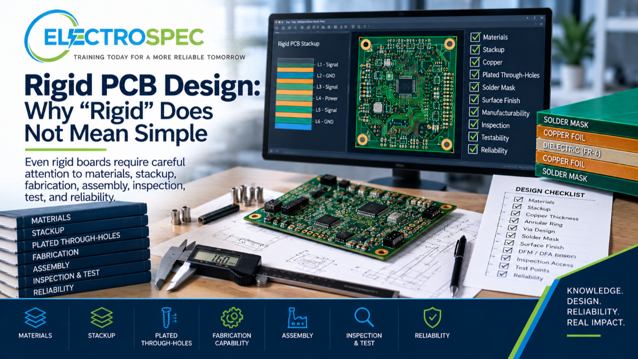
Rigid printed circuit boards are common.
Because they are common, they are sometimes treated as simple.
That can be a mistake.
A rigid PCB may not bend like a flex circuit. It may not always require HDI structures, RF materials, or exotic construction. But rigid PCB design still requires careful engineering judgment.
Rigid boards involve materials, stackup, copper thickness, conductor spacing, plated through-holes, vias, annular ring, solder mask, surface finish, mechanical support, fabrication capability, assembly process compatibility, inspection access, testability, documentation, and reliability.
A rigid board can be simple.
But it can also be complex, high-density, high-current, high-speed, high-reliability, Class 3, aerospace, defense, medical, industrial, or harsh-environment.
The word “rigid” describes the board structure.
It does not automatically describe the design difficulty.
Rigid Boards Still Depend on Materials
Every rigid PCB begins with a material system.
The designer must understand how material choices affect fabrication, soldering, thermal behavior, electrical performance, dimensional stability, moisture resistance, and reliability.
Material considerations may include:
- laminate type
- resin system
- glass reinforcement
- dielectric thickness
- copper foil
- copper thickness
- thermal expansion
- glass transition behavior
- moisture behavior
- soldering compatibility
- surface finish compatibility
- reliability under thermal cycling
A rigid board is not just a hard platform for components.
It is an engineered material structure.
Stackup Is a Core Design Decision
Stackup is one of the most important rigid PCB design decisions.
It affects electrical performance, manufacturability, impedance, power distribution, signal integrity, thermal behavior, mechanical stiffness, cost, and supplier capability.
Designers should consider:
- layer count
- layer order
- dielectric spacing
- plane placement
- copper distribution
- controlled impedance needs
- power and ground strategy
- symmetry
- board thickness
- fabrication capability
- documentation clarity
A stackup should not be selected casually.
It should support the electrical function, manufacturing process, inspection needs, and reliability expectations of the product.
Copper Thickness Affects More Than Current
Copper thickness is often associated with current carrying capability.
That matters.
But copper thickness also affects fabrication, etching, spacing, thermal behavior, soldering, plating, impedance, and cost.
Designers should understand how copper affects:
- trace width
- current capacity
- voltage drop
- temperature rise
- etching tolerance
- conductor spacing
- thermal spreading
- solder joint heating
- copper balance
- board warpage
- fabrication yield
More copper is not always better.
Less copper is not always acceptable.
The right copper choice depends on the product requirement.
Plated Through-Holes Require Design Discipline
Plated through-holes are one of the most important reliability features in rigid PCB design.
They provide electrical interconnection through the board and may also support component leads.
Designers should consider:
- hole size
- finished hole diameter
- drill tolerance
- plating thickness
- aspect ratio
- annular ring
- lead-to-hole fit
- solder fill
- thermal relief
- board thickness
- supplier capability
- inspection requirements
- reliability under thermal cycling
A plated through-hole is not just a hole.
It is a fabricated interconnect structure.
If the design pushes fabrication limits or ignores assembly requirements, plated through-hole reliability can suffer.
Annular Ring Matters
Annular ring is a small feature with large importance.
It helps support reliable plated hole connections and manufacturing tolerance.
Designers should understand how annular ring is affected by:
- drill tolerance
- registration
- pad size
- finished hole size
- plating
- board thickness
- product class
- supplier capability
- fabrication yield
Weak annular ring decisions can affect reliability, inspection, and fabrication acceptance.
A designer should not treat annular ring as only a CAD setting.
It is part of the physical reliability of the board.
Vias Are Fabricated Structures
Vias may look simple on a layout screen, but they are real fabricated structures.
Designers should consider:
- via size
- drill size
- pad size
- aspect ratio
- plating capability
- via spacing
- thermal behavior
- current carrying needs
- signal integrity effects
- reliability
- supplier capability
For advanced rigid boards, vias may become even more important.
Dense boards, high-current boards, controlled impedance designs, high-speed products, and Class 3 applications all require more careful via decisions.
A via should be designed, not merely placed.
Solder Mask and Surface Finish Affect Manufacturing
Solder mask and surface finish are often selected late, but they should be part of the design conversation.
Solder mask affects:
- solder bridging risk
- pad definition
- solder joint formation
- inspection visibility
- cleanliness
- coating compatibility
- fabrication registration
Surface finish affects:
- solderability
- shelf life
- planarity
- contact performance
- corrosion risk
- assembly compatibility
- cost
- reliability
These are not cosmetic decisions.
They affect how the rigid board will be fabricated, assembled, inspected, and used.
Rigid Boards Still Have Mechanical Requirements
Rigid does not mean mechanically immune.
Rigid boards still experience mechanical stress.
They may be mounted, handled, transported, assembled into enclosures, connected to cables, exposed to vibration, shocked, repaired, or serviced.
Designers should consider:
- board thickness
- mounting hole placement
- support points
- component height
- heavy components
- connector loading
- board flexure
- edge clearance
- hardware clearance
- enclosure fit
- vibration exposure
- shock exposure
A rigid board can still crack solder joints, damage components, loosen connectors, or fail in the field if mechanical realities are ignored.
Rigid Boards Must Support Assembly
Rigid PCB design must support the assembly process.
The designer should understand whether the product will use:
- SMT reflow
- wave soldering
- selective soldering
- manual soldering
- press-fit installation
- cleaning
- conformal coating
- staking or bonding
- rework
Design decisions affect assembly through land patterns, component spacing, thermal relief, board finish, solder mask, copper balance, component orientation, and access.
A rigid board that is electrically correct may still be difficult to assemble.
Good rigid PCB design supports the manufacturing process.
Inspection and Test Access Still Matter
Rigid boards must be inspected and tested.
Designers should ask:
- Can solder joints be inspected?
- Are markings visible?
- Are polarity indicators clear?
- Can bottom termination components be verified?
- Is X-ray inspection needed?
- Can test points be accessed?
- Can coating be inspected?
- Can hardware installation be verified?
- Can functional test be performed?
- Can objective evidence be produced?
A rigid board does not automatically guarantee inspection or test access.
Those features must be planned.
Documentation Communicates the Rigid Board Design
The release package must clearly communicate the designer’s intent.
For rigid boards, documentation may include:
- fabrication drawing
- assembly drawing
- stackup
- material requirements
- copper thickness
- controlled impedance requirements
- hole table
- via requirements
- solder mask requirements
- surface finish
- tolerances
- product class
- inspection requirements
- test requirements
- special process notes
- revision control
A good rigid board can fail in execution if the documentation is unclear.
Manufacturing cannot build intent that was never communicated.
High-Reliability Rigid Boards Require More Care
Rigid boards used in Class 3, aerospace, defense, medical, industrial, transportation, or harsh-environment products require stronger design discipline.
Designers may need to consider:
- material reliability
- plated through-hole reliability
- solder joint fatigue
- thermal cycling
- vibration
- shock
- moisture exposure
- cleanliness
- coating compatibility
- inspection evidence
- test evidence
- qualification requirements
- customer flow-downs
- objective evidence
A rigid board may be physically stiff, but the reliability burden may still be high.
High reliability must be designed into the board.
CID Advanced Builds Rigid PCB Design Judgment
ElectroSpec’s CID Advanced track includes Rigid PCB Design because rigid boards are foundational to advanced PCB design.
The course helps designers think about rigid board requirements in the context of materials, fabrication, assembly, inspection, test, reliability, and product acceptance.
Rigid PCB design is also connected to the rest of the CID Advanced pathway, including:
- PCB Fabrication & Assembly
- PCB Materials
- Flexible PCB Design
- HDI PCB Design
- RF/Microwave PCB Design
- Environmental Stress Screening
That connection matters.
A rigid board may include HDI features.
It may support RF performance.
It may require advanced materials.
It may need Class 3 reliability.
It may face environmental stress.
Rigid PCB design is not isolated from the rest of the design system.
CID Fundamentals Provides the Base
ElectroSpec’s CID Fundamentals course gives designers the foundation needed before advanced rigid PCB design decisions become meaningful.
It includes 22+ hours of on-demand training across 12 structured modules covering materials, layout principles, mechanical and electrical considerations, thermal management, component technologies, interconnections, fabrication requirements, documentation, quality assurance, manufacturability, and standards-based design thinking.
CID Advanced then builds deeper understanding for more demanding board technologies and applications.
Better Rigid PCB Design Starts with Better Questions
Before releasing a rigid PCB design, designers should ask:
- What material system is appropriate?
- Is the stackup realistic and documented?
- Are copper thicknesses correct?
- Are conductor widths and spacings suitable?
- Are plated through-hole requirements understood?
- Are via structures within supplier capability?
- Is annular ring adequate?
- Is the solder mask strategy appropriate?
- Is the surface finish compatible with assembly and reliability?
- Can the board be assembled?
- Can the product be inspected?
- Can the product be tested?
- Can the design survive the intended environment?
- Is the release package complete and clear?
These questions help designers avoid treating rigid boards as simple by default.
Final Thought
Rigid PCB design is common.
But common does not always mean easy.
Rigid boards still require careful decisions about materials, stackup, copper, vias, plated through-holes, annular ring, solder mask, surface finish, assembly, inspection, test, documentation, and reliability.
A rigid board can be simple when the product is simple.
But when performance, density, environment, reliability, or customer requirements increase, rigid PCB design becomes a serious engineering discipline.
Rigid does not mean simple.
Rigid means the designer must understand how a physical board becomes a reliable product.
Related ElectroSpec Training
ElectroSpec’s CID Advanced training includes Rigid PCB Design as part of a specialized advanced PCB design pathway.
The CID Advanced track also includes PCB Fabrication & Assembly, PCB Materials, Flexible PCB Design, HDI PCB Design, RF/Microwave PCB Design, and Environmental Stress Screening.
Together, these courses help designers build the advanced standards-connected foundation needed for CID+ certification preparation and real-world design decisions.
Coming Next
Electrical Design Considerations Beyond the Schematic
In the next article, we will return to the CID Fundamentals track and discuss why electrical design does not stop at the schematic. PCB layout decisions affect current, voltage spacing, impedance, signal behavior, grounding, noise, power integrity, and product reliability.
IPC CID Certification — ElectroSpec
IPC CID+ Certification — ElectroSpec
IPC CID/CID+ Bundle — Complete PCB Design Certification — ElectroSpec