Thermal Management Starts in the PCB Layout
Sep 16, 2026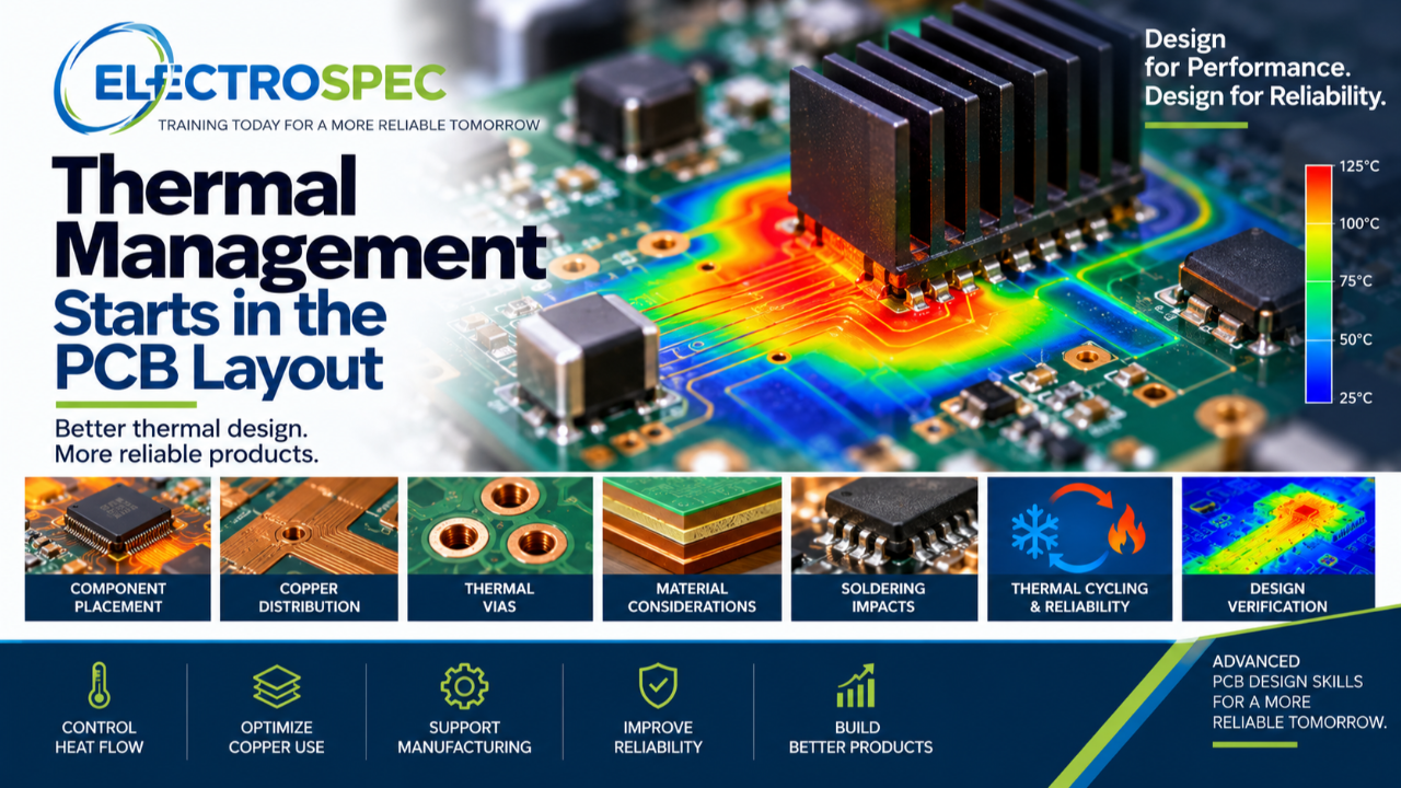
Thermal management is often treated as a component problem, enclosure problem, or system-level problem.
Those areas matter.
But thermal management also starts in the PCB layout.
A printed circuit board is not just an electrical interconnect. It is also part of the thermal path. It moves heat through copper, dielectric materials, vias, planes, pads, component terminations, mounting features, and sometimes into heat sinks, chassis, airflow, or enclosures.
A circuit may work electrically and still fail because heat was not managed properly.
That is why PCB designers must understand thermal management as part of layout.
Heat Is a Design Requirement
Heat is not an afterthought.
Every product has a thermal environment. Components generate heat, copper carries current, solder joints experience thermal stress, materials expand and contract, and the enclosure may either help or restrict heat movement.
Designers should ask:
- What parts generate heat?
- Where does the heat go?
- How does the board move heat away from the source?
- What temperature rise is acceptable?
- What materials support the thermal environment?
- What reliability risk is created by repeated heating and cooling?
Thermal performance must be designed, not assumed.
Component Placement Affects Heat
Component placement is one of the first thermal decisions in layout.
Heat-generating parts should be placed with awareness of airflow, copper area, board support, nearby heat-sensitive components, enclosure features, and assembly process effects.
Designers should consider:
- power components
- voltage regulators
- processors
- LEDs
- connectors carrying high current
- large thermal pads
- heat sinks
- temperature-sensitive components
- airflow paths
- thermal isolation needs
Poor placement can concentrate heat, reduce reliability, make soldering more difficult, or expose sensitive components to unnecessary thermal stress.
Copper Moves Heat
Copper is one of the designer’s most important thermal tools.
Copper planes, pours, traces, pads, and thermal vias can help spread and move heat. But copper also affects fabrication, soldering, impedance, current capacity, and mechanical behavior.
Designers should think about copper distribution as both an electrical and thermal decision.
A high-current trace may need wider copper to reduce temperature rise.
A power component may need copper area to spread heat.
A thermal pad may need via support to move heat into internal or opposite-side copper.
Copper balance may also affect board fabrication and assembly.
Thermal Vias Must Be Designed Carefully
Thermal vias can be useful, but they must be designed intentionally.
A via pattern under a thermal pad may help move heat, but it can also affect solder paste behavior, voiding, inspection, fabrication, and assembly yield.
Designers should consider:
- via size
- via quantity
- via placement
- via filling or plugging
- thermal pad design
- solder paste stencil design
- assembly process capability
- inspection method
- supplier capability
Thermal vias are not simply holes for heat. They are fabricated features that affect both thermal performance and assembly quality.
Soldering Is Affected by Thermal Design
Thermal layout affects soldering.
Large copper areas, heavy planes, uneven copper distribution, and high thermal mass can influence how solder joints heat during assembly.
This can affect:
- solder wetting
- through-hole fill
- reflow profile behavior
- wave solder performance
- selective soldering results
- hand soldering difficulty
- component thermal exposure
- rework risk
A designer should understand that a soldering defect may sometimes trace back to thermal imbalance in the layout.
The solder joint is formed in manufacturing, but the thermal conditions may be created in design.
Thermal Cycling Affects Reliability
Products do not always stay at one temperature.
They may heat during operation, cool when powered down, experience environmental changes, or go through qualification testing.
Thermal cycling can stress:
- solder joints
- vias
- plated through-holes
- microvias
- component terminations
- laminates
- copper interfaces
- coatings
- connectors
Different materials expand and contract at different rates. That mismatch can create fatigue over time.
For high-reliability products, thermal cycling must be considered early.
Materials Matter
Material selection affects thermal performance and reliability.
Designers should consider how materials respond to heat, including:
- thermal conductivity
- glass transition behavior
- coefficient of thermal expansion
- moisture absorption
- dimensional stability
- soldering temperature exposure
- long-term operating temperature
- thermal cycling performance
A material that works for one product may not be appropriate for a high-temperature, high-power, high-reliability, RF, HDI, or harsh-environment application.
Thermal management and material selection are connected.
Layout Must Support the Full Thermal Path
A thermal path may include the component, solder joint, pad, copper, vias, internal planes, board material, heat sink, chassis, enclosure, and airflow.
Designers should not stop at the component data sheet.
They should understand how heat actually leaves the part and moves through the product.
A weak thermal path can reduce performance, shorten component life, damage solder joints, or cause intermittent failures.
A good thermal path supports reliable operation.
Thermal Design Must Be Verified
Thermal design should be reviewed and verified.
Depending on the product, verification may include analysis, simulation, thermal imaging, temperature measurement, functional testing, environmental testing, or qualification testing.
Designers should plan how thermal performance will be proven.
If the product must meet a temperature requirement, the layout should support measurement and evidence.
CID Builds Thermal Awareness
ElectroSpec’s CID Fundamentals course includes thermal management because PCB designers need to understand how layout decisions affect heat flow, soldering, reliability, and product life.
The course provides 22+ hours of self-paced, on-demand PCB design training across 12 structured modules covering materials, layout principles, mechanical and electrical considerations, thermal management, component technologies, interconnections, fabrication requirements, documentation, quality assurance, manufacturability, and standards-based design thinking.
Thermal design is part of that foundation.
Final Thought
Thermal management does not begin after the board is built.
It begins in design.
Component placement, copper distribution, thermal vias, materials, soldering behavior, board construction, airflow, enclosure interaction, and environmental stress all affect thermal performance.
A strong PCB designer does not only ask whether the circuit works.
A strong PCB designer asks whether the product can operate reliably at temperature over time.
That is why thermal management starts in the PCB layout.
Related ElectroSpec Training
ElectroSpec’s CID Fundamentals course provides 22+ hours of self-paced, on-demand PCB design training across 12 structured modules.
The course helps designers build a standards-connected foundation in materials, layout, mechanical and electrical considerations, thermal management, fabrication, documentation, manufacturability, quality, and design decision-making while preparing for CID certification.
Coming Next
HDI PCB Design: Density, Microvias, and Fabrication Risk
In the next article, we will return to the CID Advanced track and discuss why HDI design is more than dense routing. HDI decisions affect microvias, stackup, fabrication capability, inspection, cost, and reliability.