Through-Hole Design: Wave Solder, Selective Solder, and Process Reality
Jul 27, 2026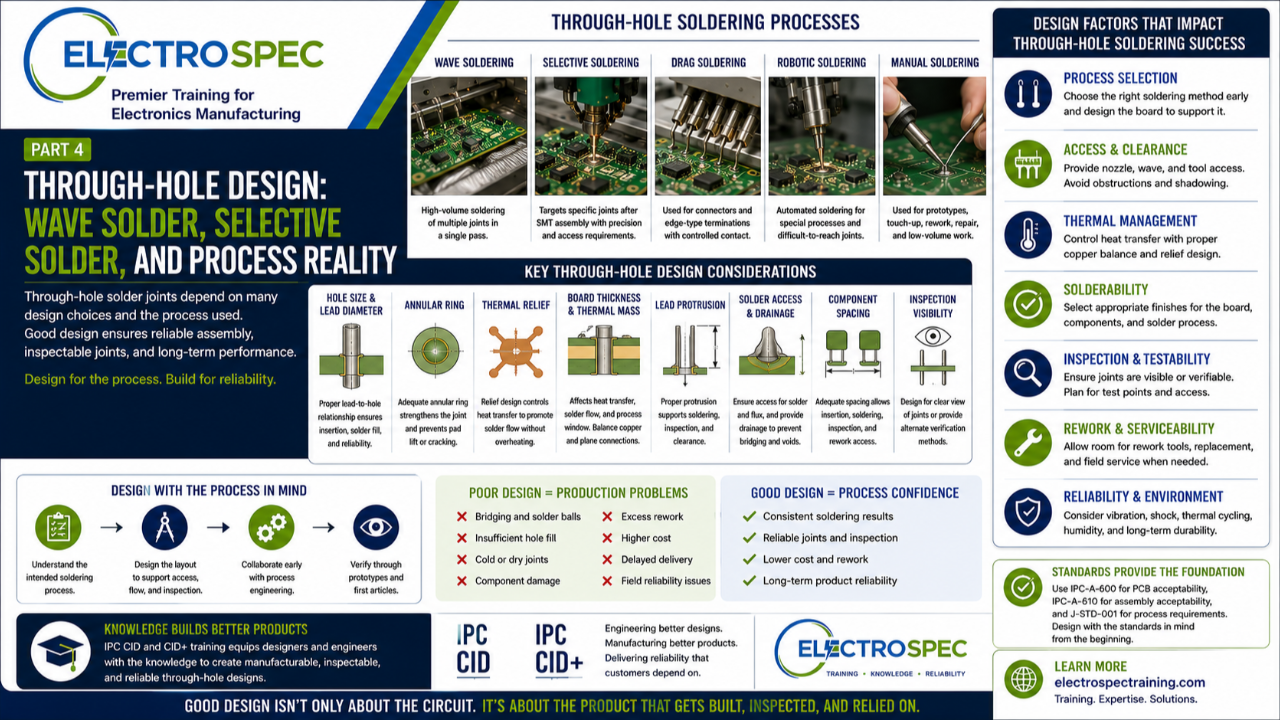
In the previous article, we discussed why SMT assembly is not hand soldering and why training must match the actual manufacturing process.
The same principle applies to through-hole technology.
Through-hole solder joints may look simple compared with fine-pitch SMT, BGAs, bottom termination components, or high-density assemblies.
But through-hole design is not simple.
A through-hole solder joint can be affected by hole size, lead diameter, board thickness, copper distribution, thermal relief, component spacing, flux access, solder access, drainage, lead protrusion, and inspection visibility.
That means designers cannot treat through-hole features as an afterthought.
Through-hole design must match the manufacturing process.
Through-Hole Is Not One Process
Through-hole soldering can be performed several different ways.
Common methods include:
- Wave soldering
- Selective soldering
- Drag soldering
- Robotic soldering
- Manual soldering
Each method has different design needs.
A board that can be hand soldered may not be well suited for wave soldering.
A board that can be selectively soldered may require spacing, keep-outs, and nozzle access that were not considered during layout.
A connector that looks acceptable in CAD may become difficult to solder consistently if the board thickness, thermal mass, or access constraints were not considered.
The soldering process matters.
Wave Soldering Requires Process-Friendly Layout
Wave soldering is often used when many through-hole joints must be soldered efficiently.
But the design must support the process.
Designers and process engineers must consider:
- Board orientation
- Component shadowing
- Wave direction
- Flux application
- Preheat requirements
- Solder contact time
- Lead protrusion
- Drainage
- Bridging risk
- Component spacing
- Thermal relief
- Board support
- Mixed-technology concerns
When the layout does not support wave soldering, manufacturing may experience bridging, skips, insufficient hole fill, icicles, solder balls, or inconsistent results.
Those issues may appear in production, but many of them begin in design.
Selective Soldering Requires Access
Selective soldering can be extremely useful for mixed-technology assemblies, especially when only certain through-hole components need to be soldered after SMT assembly.
However, selective soldering requires access.
The nozzle must be able to reach the joint.
There must be enough clearance around the soldering location.
Nearby components, connectors, tall parts, fixtures, and board features can interfere with the process.
Designers should consider:
- Nozzle diameter
- Keep-out areas
- Component-to-component spacing
- Connector body clearance
- Board edge clearance
- Bottom-side component placement
- Thermal mass
- Flux targeting
- Preheat and dwell time
- Solder flow and drainage
- Inspection visibility
A design that does not provide access may force the manufacturer into manual soldering, rework, or special tooling.
That adds cost and risk.
Manual Soldering Has a Place, But It Should Not Be the Default Fix
Manual soldering is important for certain operations.
It may be needed for prototypes, low-volume work, touch-up, rework, repair, engineering changes, wires, terminals, or special assembly conditions.
But manual soldering should not automatically become the solution for every through-hole design problem.
Manual soldering is labor-intensive.
It depends heavily on operator skill, tool control, heat transfer, dwell time, flux activity, solder volume, cleaning, and inspection.
If a production design repeatedly requires manual soldering because the layout does not support wave or selective soldering, the issue may not be operator training.
The issue may be design for manufacturability.
Hole Size and Lead Diameter Matter
One of the most important through-hole design considerations is the relationship between the component lead and the plated through-hole.
If the hole is too small, insertion can become difficult or damaging.
If the hole is too large, solder fill and joint geometry may become inconsistent.
The design must consider:
- Lead diameter
- Lead shape
- Hole diameter
- Plating thickness
- Fabrication tolerance
- Component tolerance
- Insertion method
- Solder fill expectations
- Venting and solder flow
- Rework considerations
A proper lead-to-hole relationship supports assembly, solder flow, inspection, and reliability.
A poor relationship can create production problems that are difficult to correct later.
Board Thickness and Thermal Mass Matter
Through-hole soldering is affected by heat transfer.
Thick boards, heavy copper, large planes, connectors, shielding, and high thermal mass components can make soldering more difficult.
If the assembly cannot heat properly, solder may not flow through the barrel as intended.
If the design pulls heat away too aggressively, the process engineer may need higher temperatures or longer dwell times, which can increase risk elsewhere on the assembly.
Designers should consider:
- Board thickness
- Copper weight
- Plane connections
- Thermal relief
- Component thermal mass
- connector mass
- heat sinking
- nearby components
- laminate limitations
- process window
Thermal management is not only a field-performance issue.
It is also a manufacturing issue.
Thermal Relief Is a Design Decision
Thermal relief can make through-hole soldering more consistent by reducing excessive heat sinking into large copper areas.
Without adequate thermal relief, solder may not wet or flow as expected.
With inappropriate thermal relief, the design may create electrical, thermal, or reliability concerns.
This is where engineering judgment matters.
The designer must balance electrical performance, thermal performance, manufacturability, and reliability.
That balance should be made deliberately, not discovered during production failures.
Lead Protrusion and Inspection Matter
Lead protrusion is not just a visual detail.
It affects solder joint formation, inspection, clearance, and reliability.
Designers should consider whether the selected component, board thickness, and assembly method will produce acceptable lead protrusion for the intended class and acceptance requirements.
Inspection also matters.
If the solder joint cannot be seen, measured, or otherwise verified, the manufacturer must have another acceptable method to demonstrate conformance.
Designers should ask:
- Can the joint be inspected?
- Is there enough visibility?
- Is magnification required?
- Will AOI be useful?
- Is manual inspection practical?
- Will nearby components block the view?
- Can rework be performed if needed?
Designing for inspection prevents problems after the product is built.
Component Spacing Affects Soldering and Rework
Component spacing is often treated as a layout density issue.
It is also a manufacturing issue.
Through-hole components need enough space for:
- insertion
- tooling
- solder flow
- nozzle access
- flux access
- cleaning
- inspection
- rework
- repair
- strain relief where applicable
When components are packed too tightly, manufacturing may be forced into slower, more difficult, and less repeatable methods.
That increases cost and risk.
Mixed-Technology Boards Require Extra Planning
Many modern assemblies include both SMT and through-hole components.
That creates additional process planning challenges.
For example:
- SMT components may already be installed before through-hole soldering.
- Bottom-side SMT components may interfere with wave or selective soldering.
- Large connectors may require selective soldering after reflow.
- Temperature-sensitive components may limit thermal profiles.
- Cleaning requirements may become more complicated.
- Rework access may be reduced.
Designers should understand the intended assembly sequence before the layout is finalized.
A mixed-technology board should be designed for the actual process flow, not just the electrical schematic.
Process Engineers Should Be Involved Early
Through-hole manufacturability improves when process engineers are involved before design release.
Process engineers can help evaluate:
- wave solder suitability
- selective solder access
- fixture requirements
- solderability risks
- component spacing
- thermal concerns
- rework access
- inspection approach
- cleaning constraints
- process window
This feedback is most valuable early.
Once the design is released and hardware is built, changes become more expensive and disruptive.
Designers Must Understand Acceptance Criteria
Inspectors commonly use IPC-A-610 to evaluate completed electronic assemblies.
J-STD-001 may define soldering process and workmanship requirements.
Designers should understand the acceptance expectations that the final product must meet.
They do not need to become production operators, but they should understand how design choices affect:
- solder fill
- wetting
- fillet formation
- lead protrusion
- component mounting
- cleanliness
- spacing
- damage
- inspection access
- rework feasibility
Designing without understanding acceptance criteria creates unnecessary risk.
Final Thought
Through-hole design must match the manufacturing process.
Wave soldering, selective soldering, drag soldering, robotic soldering, and manual soldering each have different requirements.
A good through-hole design supports solder access, thermal control, solder flow, lead protrusion, inspection, rework, and long-term reliability.
The solder joint may be formed in manufacturing, but the conditions for success are established during design.
Designers who understand process reality create products that are easier to build, easier to inspect, and more likely to perform reliably in the field.
Related ElectroSpec Training
ElectroSpec’s IPC CID and CID+ training programs help PCB designers and product engineers understand how design decisions affect fabrication, assembly, soldering, inspection, and reliability.
ElectroSpec’s High-Reliability Soldering & Rework training helps process engineers and manufacturing teams understand soldering processes, workmanship expectations, and reliability concerns.
ElectroSpec also offers IPC-A-610 certification for personnel who need to understand electronic assembly acceptance criteria.
Coming Next
Designers Must Understand IPC-A-610 Even If They Are Not Inspectors
In the next article, we will explain why designers benefit from understanding final product acceptance criteria, even when they are not responsible for performing inspection.
Related Reading
- Why Solder Joint Reliability Starts with Design, Not the Soldering Operator
- SMT Assembly Is Not Hand Soldering: Why Training Must Match the Process
- Why Designers Must Design for the Manufacturing Process