Why PCB Designers Must Understand Materials Before Layout
Sep 08, 2026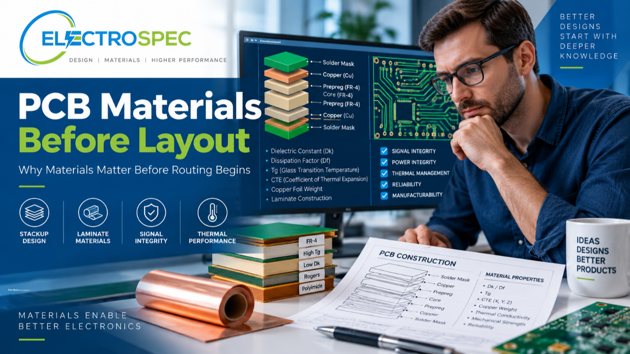
PCB layout does not begin with routing.
It begins with understanding what the board is made of.
A printed circuit board is not just copper traces on a green surface. It is an engineered material system made up of laminates, copper, resin, glass reinforcement, solder mask, surface finish, plated holes, vias, markings, and sometimes coatings, adhesives, stiffeners, or specialty materials.
Those materials affect how the board is fabricated.
They affect how the board is assembled.
They affect soldering, inspection, test, qualification, and long-term reliability.
That is why strong PCB designers must understand materials before layout begins.
Materials Are Design Decisions
Material selection is sometimes treated as a fabrication detail.
That is a mistake.
Materials directly affect design performance and manufacturability.
They influence:
- electrical behavior
- mechanical strength
- thermal performance
- solderability
- dimensional stability
- moisture resistance
- impedance control
- plating reliability
- flexural performance
- coating compatibility
- fabrication yield
- long-term reliability
A designer who does not understand materials may still create a layout that looks correct in CAD, but the board may be difficult to fabricate, difficult to assemble, or less reliable in service.
Good layout depends on good material understanding.
The Board Is More Than FR-4
Many designers casually refer to PCB material as FR-4.
But that does not tell the whole story.
There are many laminate systems, resin systems, glass styles, copper types, dielectric thicknesses, and material performance levels.
Different products may require different material considerations.
A simple commercial product may have different needs than a high-speed product, RF product, flex circuit, HDI board, Class 3 assembly, aerospace product, defense product, medical device, or harsh-environment system.
The designer must understand the product’s use environment before selecting or approving materials.
Dielectric Behavior Affects Electrical Performance
PCB materials influence electrical performance.
Dielectric constant, loss tangent, material thickness, resin content, glass weave, and copper surface characteristics can all affect how signals behave.
This becomes especially important in:
- high-speed digital designs
- RF and microwave designs
- controlled impedance designs
- dense multilayer boards
- low-loss applications
- high-frequency interconnects
- products with tight performance margins
A trace does not perform in isolation.
It performs inside a material system.
That means material selection and stackup decisions must be part of the electrical design conversation.
Thermal Behavior Affects Reliability
Materials also affect thermal performance.
Printed boards experience heat during assembly and during operation.
They may also experience thermal cycling in the field.
Different materials expand and contract differently. That mismatch can create stress in copper features, plated through-holes, vias, solder joints, components, and laminate structures.
Designers should consider:
- coefficient of thermal expansion
- glass transition temperature
- decomposition temperature
- operating temperature
- assembly temperature exposure
- thermal cycling
- copper distribution
- board thickness
- component heat generation
- heat flow paths
Thermal behavior is not only a reliability topic.
It is a design topic.
Copper Matters
Copper is not just the conductor.
Copper affects current carrying capability, voltage drop, heat spreading, impedance, fabrication limits, plating, etching, solderability, and mechanical reliability.
Designers should understand:
- copper weight
- copper thickness
- copper balance
- copper roughness
- internal versus external copper
- plated copper
- copper distribution
- current requirements
- thermal effects
- fabrication capability
A current-carrying trace, an RF trace, a controlled impedance trace, and a thermal copper area may all require different design thinking.
Copper is part of the electrical, thermal, mechanical, and manufacturing system.
Materials Affect Fabrication Capability
The fabricator must turn the design into a real board.
Material choices influence how the board can be drilled, plated, etched, laminated, finished, inspected, and controlled.
Material and fabrication decisions affect:
- line width
- spacing
- drill quality
- hole plating
- via reliability
- layer registration
- controlled impedance
- solder mask adhesion
- surface finish quality
- bow and twist
- dimensional stability
- manufacturing yield
A material may look good on paper but still create fabrication or supply chain challenges.
That is why designers should understand both material performance and supplier capability.
Materials Affect Assembly
Materials also affect assembly.
The board must survive soldering and other manufacturing processes.
Designers should think about how materials interact with:
- solder paste printing
- reflow soldering
- wave soldering
- selective soldering
- manual soldering
- cleaning
- conformal coating
- staking or bonding
- rework
- inspection
- test
A board material that cannot tolerate the process well may create defects, delamination, poor solderability, warpage, or reliability concerns.
A designer does not need to operate every soldering process, but the designer should understand how material choices affect assembly outcomes.
Surface Finish Is a Material Decision
Surface finish is sometimes selected late, but it should be considered early.
Surface finish affects solderability, shelf life, planarity, contact performance, corrosion risk, inspection, cost, and compatibility with the assembly process.
Different finishes may be appropriate for different products, depending on:
- component types
- soldering process
- storage time
- fine-pitch features
- wire bonding needs
- connector contact requirements
- reliability expectations
- customer requirements
- environmental exposure
Surface finish is not just a board shop preference.
It is a design and reliability decision.
Solder Mask and Legend Matter
Solder mask helps define exposed copper, solderable areas, protection, and assembly behavior.
Legend and markings help communicate component orientation, polarity, reference designators, revision details, and inspection information.
These features affect:
- solder joint formation
- solder bridging risk
- inspection visibility
- assembly communication
- polarity verification
- rework
- traceability
- cleanliness
- coating compatibility
A designer who ignores solder mask and legend may create avoidable manufacturing and inspection problems.
Small documentation details can create large production consequences.
Material Choices Affect High-Reliability Products
For Class 3, aerospace, defense, medical, industrial, transportation, and harsh-environment products, materials become even more important.
Designers may need to consider:
- thermal cycling resistance
- moisture resistance
- vibration and shock exposure
- long service life
- solder joint fatigue
- plated through-hole reliability
- outgassing concerns
- coating compatibility
- cleanliness requirements
- controlled process evidence
- customer flow-downs
- qualification requirements
High reliability is not created by a label.
It is built through material choices, design choices, fabrication capability, assembly control, inspection, test, and objective evidence.
CID Builds the Material Foundation
ElectroSpec’s CID Fundamentals course helps designers understand why materials matter before layout begins.
The course includes 22+ hours of on-demand PCB design training across 12 structured modules covering materials, layout principles, mechanical and electrical considerations, thermal management, component technologies, interconnections, fabrication requirements, documentation, quality assurance, manufacturability, and standards-based design thinking.
Materials are part of that foundation because every PCB design decision eventually becomes a physical product.
A designer who understands materials can make better decisions about stackup, copper, spacing, routing, thermal behavior, fabrication, assembly, and reliability.
Material Knowledge Supports Better Questions
A strong designer asks better questions before release:
- What material system is appropriate for the product?
- What environment will the board experience?
- What thermal exposure must the board survive?
- What copper thickness is required?
- What stackup supports performance and fabrication?
- What surface finish is appropriate?
- What solder mask requirements apply?
- What supplier capability limits matter?
- What documentation is needed?
- What evidence will prove conformance?
These questions help move the designer from layout activity to engineering judgment.
Final Thought
PCB materials are not background information.
They are part of the design.
The layout only works if the material system supports the electrical, mechanical, thermal, manufacturing, and reliability needs of the product.
A designer who understands materials before layout can make better decisions, communicate better with suppliers, reduce manufacturing risk, and build more reliable products.
Good PCB design does not begin with a trace.
It begins with understanding the board itself.
Related ElectroSpec Training
ElectroSpec’s CID Fundamentals course provides 22+ hours of self-paced, on-demand PCB design training across 12 structured modules.
The course helps designers build a standards-connected foundation in materials, layout, fabrication, documentation, manufacturability, quality, and design decision-making while preparing for CID certification.
Coming Next
PCB Fabrication and Assembly Realities for Advanced Designers
In the next article, we will shift to the CID Advanced track and discuss why advanced designers must understand fabrication and assembly realities before making design decisions that affect cost, yield, reliability, inspection, and certification preparation.
IPC CID Certification — ElectroSpec
IPC CID+ Certification — ElectroSpec
IPC CID/CID+ Bundle — Complete PCB Design Certification — ElectroSpec