The Designer as Engineer and Artist: Standards Give the Rules, Creativity Builds the Product
Aug 23, 2026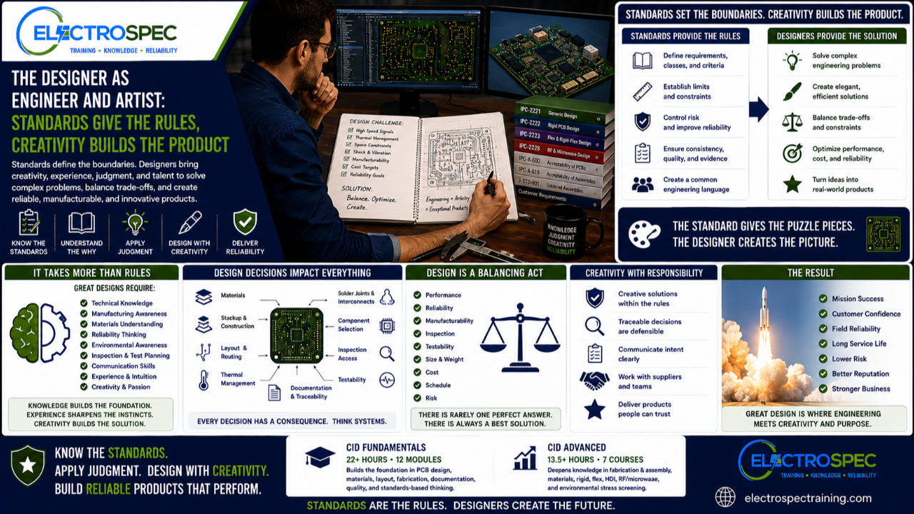
PCB design is both technical and creative.
It requires standards, requirements, rules, materials knowledge, manufacturing awareness, inspection planning, and reliability thinking.
But it also requires imagination.
It requires judgment.
It requires the ability to see the solution before the product exists.
That is why the strongest PCB designers are not just rule followers.
They are engineers and artists.
Standards provide the rules.
Designers create the product.
Standards Define the Boundaries
Standards are essential.
They help define what must be considered in the design.
They support requirements for:
- materials
- spacing
- conductors
- stackup
- board construction
- fabrication
- assembly
- soldering
- inspection
- documentation
- reliability
- qualification
- objective evidence
Without standards, design decisions become more subjective. Suppliers may interpret requirements differently. Inspectors may disagree. Customers may lack confidence. Manufacturing teams may struggle to understand design intent.
Standards create structure.
They create a common language.
They help define the boundaries of acceptable design and manufacturing practice.
But boundaries are not the same as creativity.
The Standard Does Not Create the Design
A standard can tell the designer what must be considered.
It can tell the designer what risks must be controlled.
It can define requirements, limits, classes, criteria, and expectations.
But the standard does not decide the final layout.
It does not select the exact component placement.
It does not choose the best routing strategy.
It does not solve the thermal problem.
It does not balance cost, size, reliability, manufacturability, inspection, and customer requirements.
The designer does that.
A standard gives the designer the rules of the game.
The designer still has to play the game well.
Standards Are the Puzzle Pieces
One of the best ways to understand PCB design is to think of it as a puzzle.
Standards provide the puzzle pieces.
The designer creates the picture.
The pieces have rules.
They must fit together in certain ways.
Materials must support the environment.
Spacing must support electrical and reliability needs.
Stackup must support fabrication and performance.
Routing must support signal integrity and manufacturability.
Assembly must support soldering and inspection.
Documentation must support production and objective evidence.
But the final picture is not created by the pieces alone.
The designer decides how everything comes together.
That is the creative act of engineering.
Design Is Like Boolean Logic
Boolean logic has rules.
The rules are fixed.
A logic expression must follow those rules.
But within those rules, engineers can create incredibly complex systems.
Computers, controls, communication systems, embedded electronics, and intelligent products can all be built from basic logical structures.
PCB design is similar.
The standards give the rules.
The designer uses those rules to create something unique.
Two designers may follow the same standards and still produce different layouts, different routing strategies, different stackups, different mechanical solutions, and different manufacturing outcomes.
The rules matter.
But the solution still comes from the designer.
Creativity Does Not Mean Ignoring Requirements
Creative design does not mean doing whatever looks good.
Creative design does not mean ignoring standards.
Creative design does not mean bypassing manufacturability.
In engineering, creativity must be responsible.
A creative PCB designer works inside the requirement framework while still finding the best practical solution.
That means balancing:
- electrical performance
- manufacturability
- inspection access
- testability
- reliability
- thermal performance
- mechanical constraints
- material availability
- supplier capability
- cost
- schedule
- customer requirements
The best designers are creative because they understand the rules well enough to solve problems within them.
Judgment Turns Rules Into Decisions
A standard may define a requirement.
But the designer still needs judgment to apply it.
The designer must decide:
- What requirement applies?
- What product class applies?
- What environment applies?
- What customer flow-downs apply?
- What standard or specification controls?
- What supplier capability is realistic?
- What tradeoffs are acceptable?
- What risks need mitigation?
- What evidence will prove conformance?
This is where training and experience matter.
A designer who only memorizes rules may struggle when the product does not fit a simple example.
A designer who understands the reason behind the rule can make better decisions.
Talent Still Matters
Training can provide tools.
Training can build knowledge.
Training can explain standards, materials, fabrication, assembly, inspection, qualification, and reliability.
But there is still a creative talent in design.
Some designers see patterns more naturally.
Some visualize the product more clearly.
Some anticipate manufacturing problems earlier.
Some balance tradeoffs more effectively.
Some find elegant solutions inside difficult constraints.
That talent can be developed and sharpened, but it cannot be replaced by a standard.
Standards help guide the designer.
They do not replace the designer.
CID Builds the Technical Foundation
ElectroSpec’s CID Fundamentals course is built to give designers the foundation they need.
The course includes 22+ hours of on-demand PCB design training across 12 structured modules covering materials, layout principles, mechanical and electrical considerations, thermal management, component technologies, interconnections, fabrication requirements, documentation, quality assurance, manufacturability, and standards-based design thinking.
That foundation matters because creativity without technical grounding can create risk.
A designer needs to understand the materials, standards, manufacturing process, and documentation requirements before making responsible design decisions.
CID helps build that foundation.
CID Advanced Expands the Designer’s Toolbox
ElectroSpec CID Advanced builds on the foundation with advanced courses in:
- PCB Fabrication & Assembly
- PCB Materials
- Rigid PCB Design
- Flexible PCB Design
- HDI PCB Design
- RF/Microwave PCB Design
- Environmental Stress Screening
These topics help designers think beyond basic layout.
Advanced design requires understanding how materials, fabrication, technology type, assembly, environment, reliability, and qualification work together.
A flex design is not just a bendable rigid board.
An RF design is not just careful routing.
An HDI design is not just dense geometry.
A Class 3 product is not just a label.
A harsh-environment product is not just a ruggedized marketing phrase.
Advanced design requires knowledge, judgment, and creativity.
Standards Traceability Makes Creativity Defensible
Creative design decisions still need traceability.
When a designer makes a decision, the designer should know the basis for that decision.
Was it based on:
- IPC design requirements?
- customer flow-downs?
- Class 3 expectations?
- NASA requirements?
- ESA requirements?
- military specifications?
- material performance?
- fabrication capability?
- assembly process limits?
- inspection or test needs?
- environmental qualification?
- engineering judgment?
Traceability does not limit creativity.
It strengthens it.
It allows the designer to explain the design basis.
It helps suppliers understand intent.
It helps inspectors verify requirements.
It helps customers trust the product.
It helps quality teams support objective evidence.
A creative solution with traceability is not just clever.
It is defensible.
The Designer Connects the Whole System
PCB design touches the entire product lifecycle.
A designer must think about:
- requirements
- standards
- materials
- fabrication
- assembly
- soldering
- inspection
- testing
- qualification
- documentation
- reliability
- field use
Each decision affects something downstream.
A board outline affects mechanical fit.
A stackup affects impedance, fabrication, and cost.
A pad design affects solder joint formation.
A via structure affects reliability.
A component placement decision affects inspection and rework.
A coating requirement affects access and process flow.
A test point decision affects verification.
A material selection affects thermal cycling, moisture, and long-term performance.
The designer is the person who connects these realities before the product is built.
Good Design Is Not Accidental
Good PCB design rarely happens by accident.
It comes from a combination of:
- clear requirements
- proper standards use
- good materials knowledge
- manufacturing awareness
- design experience
- supplier communication
- inspection planning
- test strategy
- reliability thinking
- documentation discipline
- creative problem solving
The designer must understand the rules and then create the solution.
That is why PCB design is such a demanding discipline.
It is technical, practical, and creative at the same time.
Standards Do Not Remove Tradeoffs
Even with standards, design still involves tradeoffs.
A designer may need to balance:
- density against manufacturability
- performance against cost
- thermal needs against space limits
- inspection access against miniaturization
- reliability against schedule
- material performance against availability
- advanced technology against supplier capability
- reworkability against packaging density
- customer expectations against production reality
A standard may help define the limits.
It may help identify risk.
It may help establish minimum requirements.
But it does not always choose the best answer.
That is where judgment comes in.
The Best Designers Ask Better Questions
A weak designer asks, “What rule do I have to follow?”
A stronger designer asks, “What risk is this rule controlling?”
A stronger designer asks:
- What is the product expected to do?
- What environment will it see?
- What failures would matter most?
- What requirement applies?
- What evidence will prove conformance?
- Can the supplier build it?
- Can manufacturing assemble it?
- Can inspection verify it?
- Can the customer trust it?
- Can the product survive real use?
Those are design questions.
They are also business questions, reliability questions, and customer confidence questions.
The Designer’s Creative Responsibility
The designer’s creativity carries responsibility.
A creative layout that cannot be fabricated is not a good design.
A compact layout that cannot be inspected is not a complete design.
A high-performance design that cannot survive the environment is not reliable.
A clever design that cannot be documented or verified creates risk.
Responsible creativity creates products that are not only functional, but manufacturable, inspectable, testable, reliable, and traceable.
That is the kind of creativity strong standards-based training should support.
Independently Developed by ElectroSpec
ElectroSpec’s CID and CID Advanced courses are independently developed by ElectroSpec.
They are not IPC-authorized training and they are not official IPC curriculum.
ElectroSpec developed these courses to provide practical, standards-connected, manufacturing-aware design training for students preparing for CID and CID+ certification.
The goal is not to replace design creativity.
The goal is to give designers the technical foundation to use that creativity responsibly.
Final Thought
Standards are essential.
They provide the rules, boundaries, requirements, and reliability framework.
But standards do not create the product.
Designers do.
The designer brings creativity, judgment, experience, talent, and responsibility to the design process.
The standard gives the puzzle pieces.
The designer creates the picture.
That is why CID and CID Advanced matter.
They help designers know the standards, understand the requirements, apply the knowledge, and create better products.
Related ElectroSpec Training
ElectroSpec’s CID Fundamentals course provides 22+ hours of on-demand PCB design training across 12 structured modules.
ElectroSpec’s CID Advanced training expands into PCB Fabrication & Assembly, PCB Materials, Rigid PCB Design, Flexible PCB Design, HDI PCB Design, RF/Microwave PCB Design, and Environmental Stress Screening.
Together, these courses help designers build the standards-connected foundation needed for CID and CID+ certification preparation.
Series Wrap-Up
This series covered:
- Design standards do not replace design judgment
- Why IPC-2221 is the foundation for PCB design
- Why rigid, flex, RF, and HDI require more than one design standard
- The supporting standards PCB designers cannot ignore
- Why designers should understand J-STD-001, IPC-A-610, and IPC-A-600
- Why aerospace and defense are not requirements by themselves
- Where NASA, military, ESA, IEC, and IPC standards fit
- Why Class 3 and high reliability are more than labels
- Designing for environmental stress, qualification, and harsh environments
- The designer as engineer and artist
The message is simple:
Know the standards. Apply the knowledge. Use judgment. Create the product.
IPC CID Certification — ElectroSpec
IPC CID+ Certification — ElectroSpec
IPC CID/CID+ Bundle — Complete PCB Design Certification — ElectroSpec