Layout Principles: More Than Placing Parts and Routing Traces
Sep 10, 2026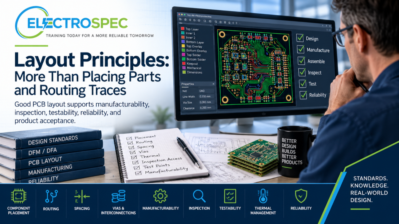
PCB layout is often described as placing components and routing traces.
That is part of the job.
But good PCB layout is much more than that.
A layout is where electrical design, mechanical constraints, materials, fabrication capability, assembly process, inspection access, testability, thermal management, documentation, and reliability all come together.
A board may be electrically correct and still be difficult to build.
It may pass design rule checks and still be difficult to inspect.
It may route cleanly and still create reliability risk.
That is why layout principles matter.
Strong layout is not only about connecting nets.
It is about creating a product that can be manufactured, inspected, tested, accepted, and trusted.
Layout Is Where Design Becomes Physical
The schematic defines electrical intent.
The layout turns that intent into a physical product.
That transition is critical.
Once components are placed, traces are routed, vias are selected, copper is distributed, and mechanical features are defined, the design begins to take on manufacturing consequences.
Layout decisions affect:
- fabrication yield
- assembly process capability
- solder joint formation
- inspection access
- test access
- thermal behavior
- mechanical support
- signal performance
- reliability
- cost
- schedule
A layout is not simply artwork.
It is an engineering decision record.
Component Placement Drives the Entire Design
Component placement is one of the most important layout decisions.
Placement affects routing, soldering, thermal performance, inspection, test, mechanical fit, rework, and product reliability.
Designers should consider:
- signal flow
- power flow
- connector locations
- mechanical constraints
- component orientation
- thermal sources
- sensitive components
- heavy or tall components
- assembly sequence
- inspection access
- test access
- rework access
- polarity visibility
- spacing for manufacturing
Poor placement can force difficult routing, create soldering problems, block inspection, complicate test, or increase reliability risk.
Good placement makes the rest of the design easier.
Routing Is More Than Connecting Points
Routing connects the circuit, but routing also affects performance and manufacturability.
A designer must consider:
- conductor width
- conductor spacing
- current carrying needs
- voltage spacing
- impedance control
- return paths
- via use
- layer transitions
- noise and coupling
- thermal effects
- fabrication limits
- inspection concerns
- reliability
A trace is not just a line.
It is a physical conductor that must carry current, survive fabrication, tolerate environmental stress, and support the product’s electrical performance.
Routing must be intentional.
Spacing Is a Design, Manufacturing, and Reliability Issue
Spacing is often treated as a design rule check item.
But spacing affects more than software compliance.
Spacing may affect:
- electrical isolation
- voltage performance
- fabrication capability
- solder bridging risk
- cleanliness
- coating coverage
- inspection access
- rework access
- long-term reliability
A spacing decision should not be based only on a default rule in the design tool.
It should be tied to the product requirements, applicable standards, supplier capability, operating environment, and customer expectations.
A strong designer understands why the spacing exists.
Vias and Interconnections Need Judgment
Vias help connect layers, but via choices affect fabrication, cost, reliability, signal behavior, inspection, and assembly.
Designers should consider:
- via size
- drill size
- aspect ratio
- annular ring
- plated through-hole reliability
- blind vias
- buried vias
- microvias
- via-in-pad
- thermal vias
- current capacity
- impedance effects
- supplier capability
A via may look simple in CAD, but it becomes a fabricated structure with real process limits.
The designer should understand how interconnections are built and how they can fail.
Layout Must Support Manufacturing
Good layout supports the manufacturing process.
The design should be compatible with the intended fabrication and assembly methods.
That may include:
- SMT reflow
- wave soldering
- selective soldering
- manual soldering
- press-fit installation
- cleaning
- conformal coating
- staking or bonding
- inspection
- test
- rework, when allowed
A layout that ignores manufacturing may create defects even if the electrical design is correct.
Manufacturability should be considered during layout, not after release.
Layout Must Support Inspection
Inspection access should be planned early.
Designers should ask:
- Can solder joints be inspected?
- Are component markings visible?
- Are polarity indicators visible?
- Are reference designators useful?
- Can bottom termination components be verified?
- Is X-ray inspection needed?
- Can coating be inspected?
- Can hardware installation be verified?
A layout that cannot be inspected creates acceptance risk.
If the design limits visual access, the inspection strategy must be considered before release.
Layout Must Support Testability
Testability is also a layout responsibility.
A product may function in theory but still be difficult to verify in production.
Designers should consider:
- test point access
- programming access
- connector access
- boundary scan
- in-circuit test
- functional test
- diagnostic points
- fixture access
- environmental test monitoring
- failure isolation
A layout that does not support test can create production delays, weak troubleshooting capability, and poor objective evidence.
Test access should not be an afterthought.
Layout Affects Thermal Performance
Thermal management is not only a component selection problem.
Layout has a major effect on how heat moves through the product.
Designers should consider:
- copper distribution
- thermal vias
- plane connections
- component spacing
- heat-producing components
- airflow
- board thickness
- material selection
- mounting surfaces
- thermal relief
- solder joint heating during assembly
Poor thermal layout can affect performance, reliability, soldering, and service life.
Good thermal layout helps protect both the product and the manufacturing process.
Layout Affects Mechanical Reliability
The PCB is also a mechanical structure.
It may be mounted, handled, flexed, vibrated, shocked, transported, repaired, or installed into an enclosure.
Designers should consider:
- board support
- mounting holes
- connector strain
- heavy components
- tall components
- edge clearance
- hardware spacing
- cable routing
- vibration exposure
- shock exposure
- service access
A layout that ignores mechanical reality can create field reliability problems.
Electrical function is not enough if the board cannot survive its physical environment.
Layout Must Communicate Design Intent
The layout must eventually be released through drawings, files, notes, and documentation.
That means layout decisions should support clear communication.
Designers should make sure the layout aligns with:
- fabrication drawings
- assembly drawings
- BOM requirements
- stackup notes
- material requirements
- surface finish requirements
- solder mask and legend
- inspection notes
- test requirements
- coating requirements
- customer flow-downs
A good layout can be weakened by poor documentation.
Design intent must be visible in the release package.
Layout Principles Support Standards Traceability
Strong layout is traceable.
When a designer makes a layout decision, the designer should understand the basis for that decision.
Is it driven by:
- an electrical requirement?
- a mechanical requirement?
- a customer requirement?
- an IPC design requirement?
- a supplier capability limit?
- an assembly process need?
- an inspection requirement?
- a test requirement?
- a reliability concern?
- engineering judgment?
Traceability helps designers explain and defend layout decisions.
It also helps manufacturing, inspection, quality, and customers understand the design intent.
CID Builds Layout Thinking
ElectroSpec’s CID Fundamentals course helps designers build practical layout knowledge as part of a broader PCB design foundation.
The course includes 22+ hours of on-demand training across 12 structured modules covering materials, layout principles, mechanical and electrical considerations, thermal management, component technologies, interconnections, fabrication requirements, documentation, quality assurance, manufacturability, and standards-based design thinking.
Layout principles are included because layout is where many design decisions become real.
A strong layout connects design intent to fabrication, assembly, inspection, test, and reliability.
Better Layout Starts with Better Questions
Before releasing a layout, designers should ask:
- Does the placement support function and manufacturing?
- Does the routing support performance and reliability?
- Are spacing rules correct and traceable?
- Are vias and interconnections appropriate?
- Can the board be fabricated reliably?
- Can the assembly process build it consistently?
- Can the product be inspected?
- Can the product be tested?
- Are thermal and mechanical concerns addressed?
- Is the release documentation clear?
These questions help move PCB layout from CAD activity to engineering discipline.
Final Thought
PCB layout is more than placing parts and routing traces.
It is where requirements, standards, materials, fabrication, assembly, inspection, test, documentation, and reliability become physical.
A strong layout supports the entire product lifecycle.
It helps the fabricator build the board.
It helps the assembler build the product.
It helps the inspector verify workmanship.
It helps the test team prove performance.
It helps the customer trust the result.
That is why layout principles are a core part of CID training.
Good layout does not only connect the circuit.
Good layout supports the product.
Related ElectroSpec Training
ElectroSpec’s CID Fundamentals course provides 22+ hours of self-paced, on-demand PCB design training across 12 structured modules.
The course helps designers build a standards-connected foundation in materials, layout, fabrication, documentation, manufacturability, quality, and design decision-making while preparing for CID certification.
Coming Next
PCB Materials for High-Reliability and Advanced Applications
In the next article, we will return to the CID Advanced track and discuss why advanced material knowledge matters for high-reliability, RF, HDI, flex, thermal, and harsh-environment PCB designs.
Related Reading
- Why PCB Designers Must Understand Materials Before Layout
- HDI and Advanced PCB Design: More Than Dense Routing
- Thermal Management Starts in the PCB Layout