Mechanical Design Considerations in PCB Design
Sep 12, 2026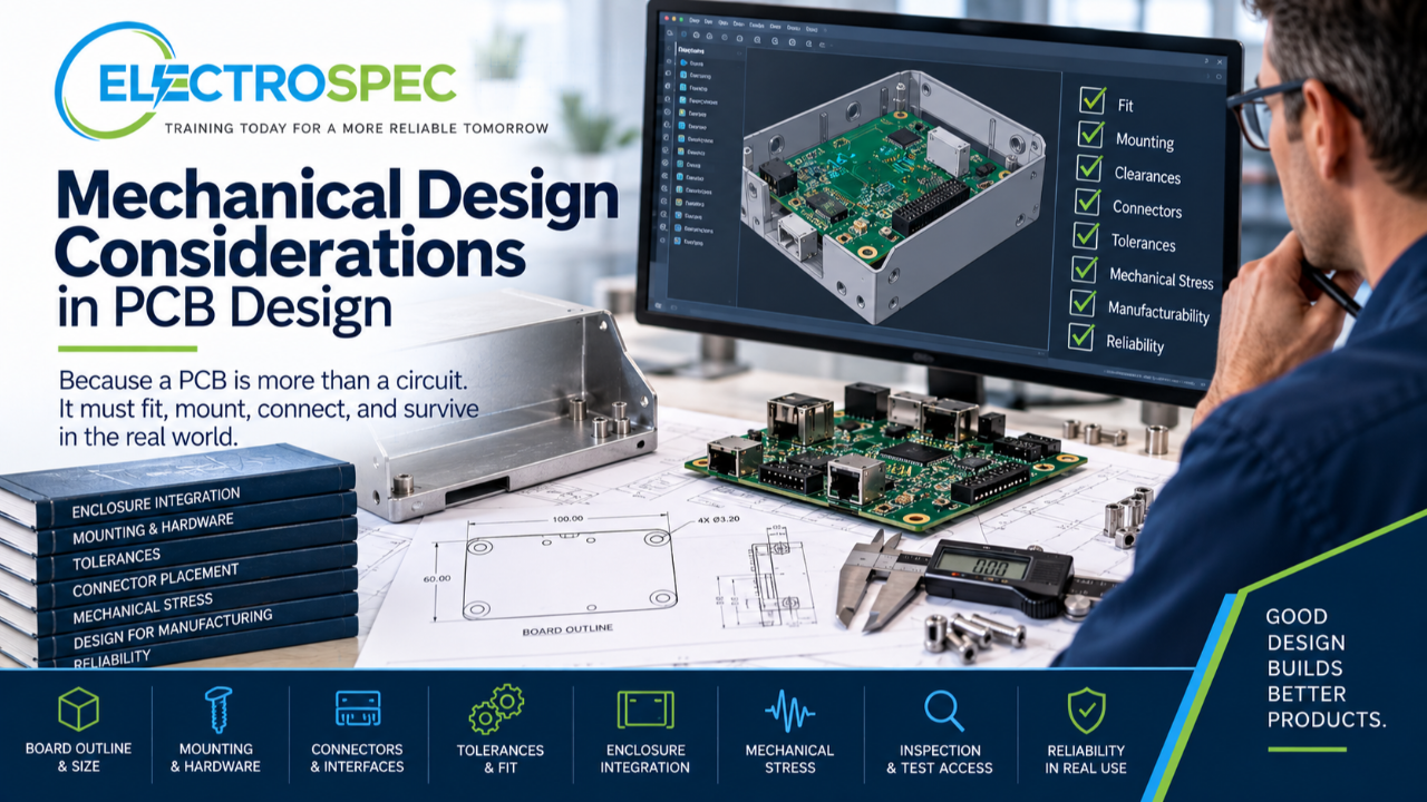
A PCB is not only an electrical circuit.
It is also a mechanical structure.
It has size, shape, thickness, weight, mounting points, connectors, hardware, clearances, tolerances, and physical interfaces. It may be installed in an enclosure, connected to cables, exposed to vibration, handled during production, repaired in the field, or required to survive shock, thermal cycling, and long-term use.
That is why PCB designers must understand mechanical design considerations.
A circuit may work electrically and still fail because the board does not fit, cannot be mounted correctly, places stress on connectors, blocks inspection access, or creates mechanical reliability risk.
Good PCB design connects electrical function with physical reality.
Board Outline Is a Design Decision
The board outline is not just a shape.
It defines how the board fits into the product.
The outline affects enclosure fit, mounting, connector placement, routing area, panelization, fabrication, assembly handling, inspection access, and serviceability.
Designers should consider:
- board size
- board shape
- edge clearances
- cutouts
- slots
- mounting holes
- connector locations
- mechanical keep-outs
- tooling features
- panelization needs
- fabrication tolerances
- assembly handling
A board outline that looks acceptable in CAD may still create problems if it conflicts with the enclosure, tooling, assembly process, or inspection method.
Mounting Holes and Hardware Matter
Mounting features are critical to mechanical reliability.
A PCB may need screws, standoffs, brackets, clips, rails, spacers, washers, or other hardware. These features affect how the board is supported and how mechanical stress moves through the assembly.
Designers should think about:
- mounting hole size
- pad and keep-out areas
- hardware clearance
- plated versus non-plated holes
- grounding requirements
- screw head clearance
- standoff location
- board support
- torque considerations
- vibration and shock loading
- service access
Poor mounting design can lead to board flexure, cracked solder joints, damaged components, connector stress, or field failures.
A board must be supported where the product needs support.
Enclosure Fit Must Be Planned Early
PCB designers should understand the enclosure before layout is finalized.
Mechanical fit affects:
- board outline
- connector locations
- component height
- keep-out areas
- mounting features
- cable routing
- heat dissipation
- airflow
- access for test
- access for service
- coating or sealing requirements
- hardware installation
A board can pass electrical testing and still be unusable if it interferes with the enclosure, cover, shield, bracket, gasket, or cable path.
ECAD and MCAD coordination can help, but the designer still needs mechanical awareness and judgment.
Component Height and Placement Affect Assembly
Component placement is not only an electrical decision.
Tall components, heavy components, connectors, transformers, relays, heat sinks, capacitors, and mechanical hardware all affect the physical design.
Designers should consider:
- maximum component height
- component-to-enclosure clearance
- component spacing
- tool access
- inspection access
- rework access
- heat sink clearance
- connector mating access
- cable strain
- vibration sensitivity
- handling risk
A tall component near an enclosure wall may create interference.
A heavy component without support may create solder joint stress.
A connector placed without access may make assembly or service difficult.
Mechanical layout choices directly affect product success.
Connectors Are Mechanical and Electrical Interfaces
Connectors are often treated as electrical components, but they are also mechanical interfaces.
They experience insertion force, removal force, cable strain, vibration, alignment pressure, handling, and service use.
Designers should consider:
- connector location
- mating direction
- cable routing
- strain relief
- mounting support
- board edge clearance
- enclosure alignment
- access for installation
- access for inspection
- retention features
- mechanical loading
A connector that is electrically correct may still fail if it is mechanically unsupported or difficult to access.
Connector placement should be reviewed with the real product use in mind.
Mechanical Stress Can Damage Electrical Reliability
Mechanical stress can create electrical failures.
Board flexure, vibration, shock, torque, connector loading, cable strain, and thermal expansion can affect solder joints, vias, components, terminations, and interconnections.
Mechanical stress may contribute to:
- cracked solder joints
- cracked ceramic components
- fractured leads
- damaged vias
- broken traces
- connector failures
- intermittent connections
- delamination
- hardware loosening
- field reliability problems
A design that ignores mechanical stress may pass initial test and fail later in real use.
Mechanical reliability must be designed into the product.
Tolerances Must Be Realistic
Tolerances are part of mechanical design.
A PCB design may include tolerances for board outline, hole location, slot size, thickness, connector placement, mounting features, panelization, and mechanical interfaces.
Designers should understand that tolerances affect fit and assembly.
They should ask:
- What tolerance is actually required?
- Can the supplier meet it consistently?
- Does the tolerance affect enclosure fit?
- Does it affect connector alignment?
- Does it affect hardware installation?
- Does it affect inspection or test fixtures?
- Does it affect cost or yield?
Overly loose tolerances may cause fit problems.
Overly tight tolerances may increase cost or supplier difficulty.
Good tolerance selection requires engineering judgment.
Keep-Outs Protect the Design
Mechanical keep-outs are essential.
They help prevent conflicts with hardware, enclosures, shields, fasteners, cables, test fixtures, coating masks, tooling, and assembly equipment.
Keep-outs may be needed for:
- mounting hardware
- screw heads
- standoffs
- enclosure walls
- connectors
- cable bends
- heat sinks
- shields
- test probes
- coating masks
- fiducials
- tooling holes
- depanelization areas
- high-voltage spacing
- service access
A missing keep-out can create expensive redesign.
Mechanical constraints should be captured early and clearly communicated in the layout and release package.
PCB Thickness Is a Mechanical Decision
Board thickness affects more than stackup.
It influences mechanical strength, connector compatibility, edge card interfaces, warpage, thermal behavior, plated through-hole reliability, vibration response, and assembly handling.
A designer should consider:
- mechanical stiffness
- connector requirements
- board support spacing
- stackup needs
- fabrication capability
- plated hole aspect ratio
- thermal performance
- weight
- enclosure fit
- assembly handling
A thin board may save space but increase flexure.
A thick board may improve stiffness but affect drilling, plating, connectors, and cost.
Thickness should be selected for the product, not by habit.
Thermal and Mechanical Design Are Connected
Thermal behavior and mechanical design often interact.
Heat sinks, thermal pads, mounting surfaces, copper planes, airflow paths, enclosures, and component spacing all affect thermal performance.
Thermal expansion also creates mechanical stress.
Designers should consider:
- heat-generating components
- thermal paths
- board support near hot components
- heat sink mounting
- airflow clearance
- enclosure conduction
- thermal cycling
- material expansion
- solder joint fatigue
- component package stress
A thermal solution that ignores mechanical support may create reliability problems.
A mechanical design that blocks airflow may create thermal problems.
The designer must think about both.
Mechanical Design Affects Manufacturing
Mechanical decisions affect fabrication and assembly.
Examples include:
- unusual board shapes
- narrow tabs
- slots and cutouts
- tight hole tolerances
- complex panelization
- heavy components
- awkward connector locations
- poor tooling access
- limited assembly clearance
- poor depanelization strategy
A design may be mechanically possible but difficult to manufacture consistently.
Designers should consider how the board will be built, handled, assembled, inspected, tested, and packaged.
Mechanical design should support manufacturing, not fight it.
Mechanical Design Affects Inspection and Test
Inspection and test access are often affected by mechanical layout.
Designers should ask:
- Can inspectors see critical areas?
- Can test probes reach test points?
- Can connectors be accessed?
- Can fixtures contact the board correctly?
- Can hardware be inspected?
- Can labels and markings be read?
- Can coating be inspected?
- Can rework tools reach the area?
- Can the product be tested inside or outside the enclosure?
If mechanical layout blocks inspection or test, the organization may struggle to prove conformance.
A design that cannot be verified creates risk.
Documentation Must Capture Mechanical Intent
Mechanical design intent must be documented clearly.
The release package may need to define:
- board outline
- hole locations
- dimensions
- tolerances
- keep-outs
- slots and cutouts
- board thickness
- hardware requirements
- connector locations
- component height limits
- assembly notes
- torque requirements
- coating keep-outs
- inspection requirements
- test fixture requirements
A good mechanical design can fail if the documentation is unclear.
Manufacturing cannot build intent that was never communicated.
Mechanical Design Supports Reliability
Reliability is not only electrical.
A reliable PCB must survive the physical conditions of the product.
That may include:
- vibration
- shock
- handling
- installation
- transportation
- thermal cycling
- connector use
- cable strain
- enclosure loading
- field maintenance
- long service life
Mechanical design choices influence whether the product survives those conditions.
A reliable product must be electrically correct and mechanically robust.
CID Builds Mechanical Awareness
ElectroSpec’s CID Fundamentals course includes mechanical design considerations because PCB designers need to understand more than electrical layout.
The course provides 22+ hours of on-demand PCB design training across 12 structured modules covering materials, layout principles, mechanical and electrical considerations, thermal management, component technologies, interconnections, fabrication requirements, documentation, quality assurance, manufacturability, and standards-based design thinking.
Mechanical awareness helps designers make better decisions before release.
It also helps designers communicate more effectively with mechanical engineers, fabricators, assemblers, inspectors, test engineers, and customers.
Better Mechanical Design Starts with Better Questions
Before releasing a PCB layout, designers should ask:
- Does the board fit the enclosure?
- Are mounting features correct?
- Are tolerances realistic?
- Are connectors supported and accessible?
- Are heavy components supported?
- Are keep-outs complete?
- Is component height controlled?
- Can the board be assembled?
- Can the product be inspected?
- Can the product be tested?
- Can the board survive vibration, shock, handling, and thermal cycling?
- Is the mechanical intent documented clearly?
These questions help prevent electrical designs from becoming mechanical failures.
Final Thought
PCB design is not only electrical design.
It is physical product design.
The board must fit, mount, connect, survive, and support the product’s intended use.
Mechanical design considerations affect manufacturability, inspection, testability, reliability, documentation, and customer acceptance.
A strong PCB designer understands that the board is both an electrical circuit and a mechanical structure.
Good design connects both.
Related ElectroSpec Training
ElectroSpec’s CID Fundamentals course provides 22+ hours of self-paced, on-demand PCB design training across 12 structured modules.
The course helps designers build a standards-connected foundation in materials, layout, mechanical and electrical considerations, fabrication, documentation, manufacturability, quality, and design decision-making while preparing for CID certification.
Coming Next
Rigid PCB Design: Why “Rigid” Does Not Mean Simple
In the next article, we will return to the CID Advanced track and discuss why rigid board design still requires careful attention to stackup, materials, fabrication capability, plating reliability, solderability, inspection, test, and product reliability.
IPC CID Certification — ElectroSpec
IPC CID+ Certification — ElectroSpec
IPC CID/CID+ Bundle — Complete PCB Design Certification — ElectroSpec