The Real Training Path for Electronics Designers
Aug 02, 2026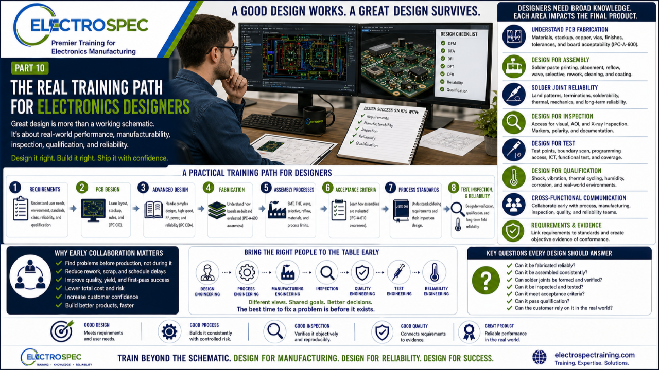
A good design is not only electrically correct. It is manufacturable, inspectable, acceptable, qualifiable, and reliable.
That idea changes how we think about designer training.
Electronics designers do not only need to understand schematics, routing, spacing, stackups, and layout tools. They also need to understand how their design decisions affect fabrication, assembly, soldering, inspection, test, qualification, and long-term product performance.
A designer does not need to become every specialist in the factory.
But a designer does need enough manufacturing knowledge to avoid creating problems that operators, process engineers, inspectors, and quality teams must later fight downstream.
Designers Need More Than Layout Software Skills
Knowing how to use a PCB design tool is important, but software skill is not the same as design competence.
A designer may know how to place components, route traces, build footprints, and generate fabrication files.
That is necessary.
But it is not enough.
Designers also need to understand:
- how printed boards are fabricated
- how assemblies are built
- how solder joints are formed
- how components are placed
- how boards are cleaned
- how assemblies are inspected
- how test access is provided
- how qualification requirements affect design
- how materials affect reliability
- how manufacturing defects are prevented
A design tool helps create the layout.
Training helps the designer understand what that layout means in the real world.
Start with Requirements
The real training path begins with requirements.
Before layout begins, the designer should understand:
- user needs
- customer requirements
- product class
- operating environment
- reliability expectations
- qualification requirements
- manufacturing volume
- inspection strategy
- test strategy
- cost and schedule constraints
- applicable standards
- customer flow-downs
A product designed for consumer electronics may not need the same design approach as a product used in aerospace, defense, medical, transportation, or critical infrastructure.
Designers must understand what the product must do, where it will be used, and how failure would affect the user.
Learn PCB Fabrication
Designers should understand printed board fabrication because PCB fabrication decisions affect yield, cost, reliability, and assembly success.
Important topics include:
- base materials
- laminate selection
- copper thickness
- board thickness
- stackup
- controlled impedance
- via structures
- plated through-holes
- annular ring
- conductor width and spacing
- solder mask
- surface finish
- panelization
- drill tolerances
- fabrication notes
- board acceptability
This is where IPC-A-600 awareness can help.
IPC-A-600 addresses printed board acceptability. Designers may not perform incoming board inspection, but they should understand what a fabricated board must meet before assembly begins.
A weak fabricated board can create problems before the first component is placed.
Learn Design for Assembly
Design for Assembly is critical because the design must support the actual assembly process.
Designers should understand how layout decisions affect:
- SMT placement
- solder paste printing
- stencil design
- reflow soldering
- through-hole insertion
- wave soldering
- selective soldering
- robotic soldering
- manual soldering
- connector installation
- mechanical hardware
- cleaning
- coating
- rework
Component location, orientation, spacing, land pattern design, thermal balance, and process access all matter.
A designer who understands assembly will avoid layouts that are technically possible but unnecessarily difficult to build.
Learn Solder Joint Formation
Solder joints are often inspected at the end, but many solder joint success factors are created in design.
Designers should understand how solder joint reliability is affected by:
- land pattern design
- pad geometry
- component termination geometry
- solder mask design
- board finish
- component finish
- stencil aperture
- solder paste volume
- placement accuracy
- reflow profile
- hole-to-lead relationship
- thermal relief
- board thickness
- lead protrusion
- mechanical support
- environmental stress
The solder joint may be formed in manufacturing, but design determines whether the process has a fair chance of producing a reliable joint.
Learn Acceptance Criteria
Designers should understand acceptance criteria because their products will eventually be judged against acceptance criteria.
IPC-A-610 is often used to evaluate completed electronic assemblies.
That does not mean every designer must become an inspector.
But designers should understand what inspectors and customers will be looking for.
Acceptance criteria may involve:
- solder joints
- component mounting
- component alignment
- spacing
- cleanliness
- marking
- hardware installation
- damage
- conformal coating
- wire and terminal conditions
- connector installation
- overall workmanship
When designers understand final acceptance expectations, they are better prepared to design products that can meet those expectations without excessive rework, subjective inspection, or marginal workmanship.
Learn Process Standards in Context
Designers should also understand process standards in context.
J-STD-001 is important because it defines requirements for soldered electrical and electronic assemblies.
However, designers usually do not need the same training emphasis as hand soldering technicians or rework operators.
A designer may need awareness of how J-STD-001 requirements affect:
- material choices
- solderability
- cleanliness
- coating
- thermal processes
- rework limitations
- workmanship requirements
- process controls
- reliability expectations
The designer does not need to become the soldering operator.
But the designer should understand how design choices affect the ability of the manufacturing process to meet soldering requirements.
Learn Design for Inspection and Test
A product that cannot be inspected or tested is difficult to accept with confidence.
Designers should understand how to provide:
- visual inspection access
- AOI compatibility
- X-ray strategy where needed
- test points
- programming access
- functional test access
- boundary scan where appropriate
- polarity visibility
- reference designator visibility
- connector access
- rework access
- marking and traceability
Designers should ask:
Can this product be verified after it is built?
If the answer is unclear, inspection and test planning should happen before release.
Learn Design for Reliability and Qualification
Reliability is not added after the product is built.
Qualification success begins in design.
Designers should understand how product performance is affected by:
- shock
- vibration
- thermal cycling
- humidity
- corrosion
- contamination
- mechanical stress
- connector strain
- cable routing
- board flexure
- solder joint fatigue
- component derating
- thermal management
- material compatibility
- coating and protection
- field handling
- storage conditions
A product may pass electrical test and still fail in the real world if reliability was not designed into the product.
Designers should understand the environment before selecting materials, components, layout structure, interconnects, and mechanical support methods.
Learn Cross-Functional Communication
Designers should not work in isolation.
A strong designer knows when to involve:
- process engineering
- manufacturing engineering
- quality engineering
- inspection
- test engineering
- reliability engineering
- suppliers
- production supervision
- customers where appropriate
The designer owns many upstream decisions, but the factory sees the real consequences of those decisions.
A cross-functional design review can prevent problems before they become production defects, audit findings, qualification failures, or field issues.
A Practical Training Path for Designers
A practical electronics designer training path may look like this:
1. Core PCB Design Knowledge
This includes layout principles, stackups, routing, spacing, fabrication outputs, materials, and documentation.
This is where IPC CID is especially valuable.
2. Advanced Design and Reliability Knowledge
This includes more complex design decisions, high-reliability considerations, manufacturability, electrical performance, material selection, and advanced layout tradeoffs.
This is where IPC CID+ becomes important.
3. Printed Board Acceptability Awareness
Designers should understand how bare printed boards are evaluated and what fabrication defects can affect assembly and reliability.
This connects to IPC-A-600 awareness.
4. Electronic Assembly Acceptance Awareness
Designers should understand how the completed assembly will be evaluated after manufacturing.
This connects to IPC-A-610 awareness or certification, depending on the role.
5. Soldering Process Awareness
Designers should understand how soldering requirements and process limitations affect manufacturability and reliability.
This connects to J-STD-001 awareness and high-reliability soldering knowledge.
6. Design for Manufacturing, Assembly, Inspection, Test, and Reliability
Designers should understand:
- DFM
- DFA
- DFI
- DFT
- DFR
- qualification planning
- environmental risk
- process capability
- inspection strategy
This is where design becomes more than layout.
It becomes product engineering.
Designers Do Not Need Every Certification
This is important.
A designer does not need every operator certification.
A designer does not need to be certified in every hands-on manufacturing task.
A designer does not need to perform every inspection operation.
But a designer should understand how those functions affect the product.
The best training path is role-based.
Designers need training that helps them make better design decisions.
Process engineers need training that helps them control manufacturing processes.
Operators need training that helps them perform actual work.
Inspectors need training that helps them verify product acceptability.
Quality engineers need training that helps them connect requirements to evidence.
One-size-fits-all training rarely matches the way electronics manufacturing actually works.
The Designer’s Final Question
Before release, a designer should ask:
- Does the circuit work?
- Can the board be fabricated reliably?
- Can the assembly be manufactured using the intended process?
- Can the solder joints be formed consistently?
- Can the product be inspected?
- Can the product be tested?
- Can the product meet acceptance criteria?
- Can the product survive qualification?
- Can the customer rely on it?
That is the real design mindset.
Final Thought
The real training path for electronics designers is not just about learning design software.
It is about understanding the full life of the product.
From requirements to fabrication.
From assembly to inspection.
From test to qualification.
From customer acceptance to real-world reliability.
Designers do not need to become operators or inspectors.
But they must understand how their decisions affect operators, inspectors, process engineers, quality teams, customers, and users.
A good design is not only electrically correct.
It is manufacturable, inspectable, acceptable, qualifiable, and reliable.
That is the standard designers should train toward.
Related ElectroSpec Training
ElectroSpec’s IPC CID and IPC CID+ training programs help PCB designers and product engineers understand how design decisions affect fabrication, assembly, manufacturability, inspection, qualification, and reliability.
ElectroSpec also offers IPC-A-610 certification, IPC-A-600 certification, and High-Reliability Soldering & Rework training for teams that need to connect design decisions to real manufacturing and acceptance outcomes.
Series Wrap-Up
This design series covered ten important topics:
- Why designers must design for the manufacturing process
- Why solder joint reliability starts with design, not the soldering operator
- Why SMT assembly is not hand soldering
- Through-hole design for wave solder, selective solder, and process reality
- Why designers must understand IPC-A-610 even if they are not inspectors
- Who really needs J-STD-001 training
- Designing for inspection
- Designing for qualification
- Why designers, process engineers, and inspectors must talk before production
- The real training path for electronics designers
The central message is simple:
Design is not finished when the circuit works. Design is finished when the product can be built, inspected, accepted, qualified, and relied upon.