The Supporting Standards PCB Designers Cannot Ignore
Aug 17, 2026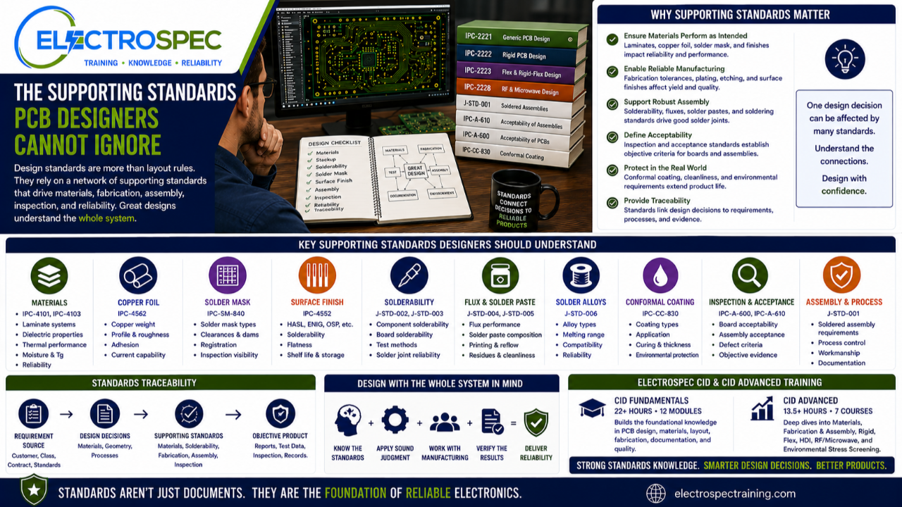
PCB design does not live inside one standard.
A designer may start with the generic design foundation, then move into rigid, flex, RF, HDI, or other technology-specific design requirements.
But even that is not the complete picture.
Real PCB design is affected by many supporting standards.
Those supporting standards address materials, fabrication, solderability, solder mask, copper foil, laminates, surface finishes, fluxes, solder pastes, solder alloys, conformal coating, assembly requirements, inspection criteria, cleanliness, documentation, reliability, and product acceptability.
That is why strong designers need more than one design standard.
They need standards literacy.
They need to understand how supporting standards affect the design before the product reaches fabrication, assembly, inspection, test, and field use.
Design Standards Do Not Stand Alone
A design standard may tell the designer how to approach the board design.
But the design will still depend on many other technical areas.
For example:
- What laminate system is being used?
- What copper foil applies?
- What solder mask is required?
- What surface finish is specified?
- What solderability requirements apply?
- What solder alloy is being used?
- What flux or solder paste is involved?
- What conformal coating will be applied?
- What assembly requirements apply?
- What inspection criteria will be used?
- What class applies?
- What environmental conditions must the product survive?
These are not separate from design.
They influence design.
A designer who ignores supporting standards may create a layout that looks correct but creates fabrication, assembly, inspection, reliability, or compliance problems later.
Materials Standards Matter
Materials are the physical foundation of the printed board.
The designer may not manufacture the laminate, copper foil, solder mask, or surface finish, but the designer’s choices affect how those materials perform.
Material-related standards and specifications may address areas such as:
- laminates and prepregs
- copper foil
- dielectric properties
- thermal expansion
- glass transition behavior
- moisture absorption
- copper adhesion
- solder mask
- marking inks
- surface finishes
- flexible circuit materials
- high-frequency materials
- high-reliability material requirements
Material selection affects electrical performance, fabrication yield, assembly processing, solderability, thermal cycling, dimensional stability, and long-term reliability.
That is why designers need to understand material requirements, not just layout geometry.
A design is not only traces and pads.
It is an engineered material system.
Laminates and Copper Foil Are Design Decisions
Laminate and copper foil choices affect the entire product.
They influence:
- impedance
- insertion loss
- thermal performance
- dimensional stability
- plating reliability
- current carrying capability
- conductor formation
- etching behavior
- soldering performance
- reliability under thermal cycling
- flexural behavior for flexible circuits
- cost and availability
For high-speed, RF, microwave, HDI, flex, aerospace, defense, medical, or harsh-environment products, material selection becomes even more important.
The wrong laminate or copper foil choice may not show up as a schematic problem.
It may show up later as yield loss, impedance variation, soldering defects, environmental failure, or field reliability issues.
That is why ElectroSpec’s CID Advanced training includes PCB Materials as a dedicated advanced course.
Solder Mask, Legend, and Surface Finish Are Not Cosmetic Details
Solder mask and surface finish are often treated casually by inexperienced designers.
They should not be.
Solder mask affects:
- solder joint formation
- solder bridging risk
- solder dam design
- mask clearance
- mask-defined versus non-mask-defined pads
- fabrication registration
- inspection visibility
- cleanliness
- coating compatibility
- long-term protection
Surface finish affects:
- solderability
- shelf life
- planarity
- wire bonding suitability
- corrosion risk
- contact performance
- assembly compatibility
- cost
- reliability
Marking and legend decisions affect identification, inspection, polarity, traceability, maintenance, and assembly communication.
These details belong in the design conversation early.
They are not simply fabrication preferences.
They can affect whether the product can be built, inspected, accepted, and serviced.
Solderability Standards Affect Design Outcomes
Solderability is often discovered too late.
A designer may think solderability is only an assembly problem, but design choices influence whether reliable solder joints can be formed.
Supporting standards such as those addressing component solderability, printed board solderability, fluxes, solder pastes, and solder alloys help define the material and process expectations behind solder joint formation.
Examples include the J-STD family of standards covering areas such as:
- soldered assembly requirements
- component solderability
- printed board solderability
- fluxes
- solder pastes
- solder alloys
Designers do not need to become solder chemists.
But they should understand that soldering performance depends on material compatibility, surface finish, component finish, land pattern design, thermal mass, assembly process, cleanliness, and process control.
The solder joint is formed in manufacturing, but many solder joint risks are created in design.
J-STD-001 and IPC-A-610 Affect Designers Too
J-STD-001 and IPC-A-610 are not design standards in the same way IPC-2221 is a design foundation.
But designers still need to understand them.
J-STD-001 addresses requirements for soldered electrical and electronic assemblies.
IPC-A-610 addresses acceptability of electronic assemblies.
Designers may not be the soldering operator or final inspector, but their decisions influence whether the assembly can meet process requirements and acceptance criteria.
Design decisions affect:
- solder joint geometry
- access for soldering
- component placement
- spacing
- thermal relief
- inspection visibility
- rework feasibility
- cleanliness
- coating
- hardware installation
- connector support
- wire and terminal interface areas
A designer who does not understand downstream assembly and acceptance standards may unintentionally create problems that appear later as defects, rework, inspection disputes, or customer concerns.
IPC-A-600 and Fabrication Acceptance Matter
Bare printed board acceptability is another area designers should understand.
A board may be designed correctly in CAD but still fail to meet fabrication acceptability expectations.
IPC-A-600 is commonly used for printed board acceptability.
Designers may not perform incoming board inspection, but they should understand what fabrication defects and acceptability concerns can affect the assembly.
Examples include:
- conductor defects
- plating concerns
- annular ring issues
- hole quality
- laminate defects
- solder mask defects
- delamination
- bow and twist
- surface finish issues
- marking issues
- cleanliness concerns
A fabricated board is the platform for the entire assembly.
If the board is weak, the assembly starts weak.
Designers should understand how fabrication requirements and acceptance expectations connect to layout and documentation.
Conformal Coating Is Not a Magic Fix
Conformal coating is sometimes treated as a protective layer that solves environmental problems after the design is complete.
That is a mistake.
Conformal coating is a design consideration.
It may affect:
- component spacing
- coating coverage
- masking
- keep-out areas
- connectors
- test points
- high-voltage areas
- inspection
- rework
- material compatibility
- cleaning requirements
- environmental protection
- customer requirements
IPC-CC-830 is often associated with conformal coating qualification and performance expectations.
But designers must understand that coating effectiveness depends on design, materials, cleanliness, process control, inspection, and the real environment.
A coating cannot fully compensate for poor design decisions, incompatible materials, contamination, or unclear requirements.
Cleanliness and Contamination Affect Reliability
Cleanliness is not only a production issue.
Designers influence cleanliness through spacing, component selection, assembly density, flux entrapment risk, bottom termination components, cleaning access, coating strategy, and documentation.
Contamination can affect:
- insulation resistance
- corrosion
- leakage current
- dendritic growth
- coating adhesion
- long-term reliability
- high-voltage performance
- harsh-environment survivability
For Class 3, aerospace, defense, medical, space, and harsh-environment products, cleanliness and contamination control may be especially important.
Designers should understand how layout choices can either support or fight the cleaning and verification process.
Supporting Standards Help Define Objective Evidence
Standards are not only about design rules.
They help define what evidence is needed.
A customer, auditor, quality engineer, or failure analysis team may ask:
- What material was specified?
- What finish was used?
- What solderability requirement applied?
- What coating requirement applied?
- What fabrication requirement applied?
- What inspection standard was used?
- What class applied?
- What objective evidence proves conformance?
Supporting standards help connect the product to evidence.
That matters because high-reliability electronics require more than good intentions.
They require traceable decisions and verifiable results.
Standards Traceability Is a Design Skill
A strong designer should be able to trace design choices to the proper source.
That source may be:
- a generic design standard
- a technology-specific design standard
- a material standard
- a fabrication performance specification
- a bare board acceptability standard
- an assembly process standard
- an assembly acceptability standard
- a solderability standard
- a coating requirement
- a customer drawing
- a contract flow-down
- a qualification plan
- engineering judgment
This is why standards literacy matters.
The designer does not need to memorize every standard.
But the designer should understand the standards ecosystem well enough to know where requirements come from and when additional information is needed.
CID and CID Advanced Build the Standards Framework
ElectroSpec’s CID Fundamentals course provides the foundation.
It includes 22+ hours of on-demand training across 12 structured modules covering materials, layout principles, mechanical and electrical considerations, thermal management, component technologies, interconnections, fabrication requirements, documentation, quality assurance, manufacturability, and standards-based design thinking.
ElectroSpec CID Advanced builds on that foundation with advanced courses in:
- PCB Fabrication & Assembly
- PCB Materials
- Rigid PCB Design
- Flexible PCB Design
- HDI PCB Design
- RF/Microwave PCB Design
- Environmental Stress Screening
That combination helps designers understand not only what standards exist, but how design decisions connect to materials, fabrication, assembly, inspection, reliability, and certification preparation.
Supporting Standards Are Where Real Products Get Complicated
Many design problems occur at the boundaries between standards.
A design may satisfy a layout rule but create a soldering problem.
A material may satisfy one need but create thermal or reliability risk.
A surface finish may support assembly but raise concerns for shelf life or contact performance.
A coating may protect the assembly but make inspection or rework difficult.
A dense layout may meet electrical needs but limit cleaning, inspection, or test access.
This is where design judgment matters.
Standards provide the information.
The designer must integrate it.
Independently Developed by ElectroSpec
ElectroSpec’s CID and CID Advanced courses are independently developed by ElectroSpec.
They are not IPC-authorized training and they are not official IPC curriculum.
ElectroSpec developed these courses to provide practical, standards-connected, manufacturing-aware design training for students preparing for CID and CID+ certification.
The purpose is not only to identify standards.
The purpose is to help designers understand how standards affect real design decisions.
Final Thought
PCB designers cannot rely on one standard alone.
The design is affected by materials, fabrication, solderability, solder mask, surface finish, soldering, inspection, coating, cleanliness, documentation, and reliability requirements.
Supporting standards help define those requirements.
They help create traceability.
They help support objective evidence.
They help connect design decisions to real manufacturing and reliability outcomes.
A strong designer does not need to memorize every document.
But a strong designer must understand that the PCB design standard is only part of the requirement system.
The real design lives where the standards connect.
Related ElectroSpec Training
ElectroSpec’s CID Fundamentals course provides 22+ hours of on-demand PCB design training across 12 structured modules.
ElectroSpec’s CID Advanced training expands into PCB Fabrication & Assembly, PCB Materials, Rigid PCB Design, Flexible PCB Design, HDI PCB Design, RF/Microwave PCB Design, and Environmental Stress Screening.
Together, these courses help designers build the standards-connected foundation needed for CID and CID+ certification preparation.
Coming Next
In the next article, we will discuss why designers are not operators or inspectors, but still need to understand how manufacturing and acceptance standards affect the products they design.
IPC CID Certification — ElectroSpec
IPC CID+ Certification — ElectroSpec
IPC CID/CID+ Bundle — Complete PCB Design Certification — ElectroSpec