Assembly and Manufacturability Awareness for PCB Designers
Sep 23, 2026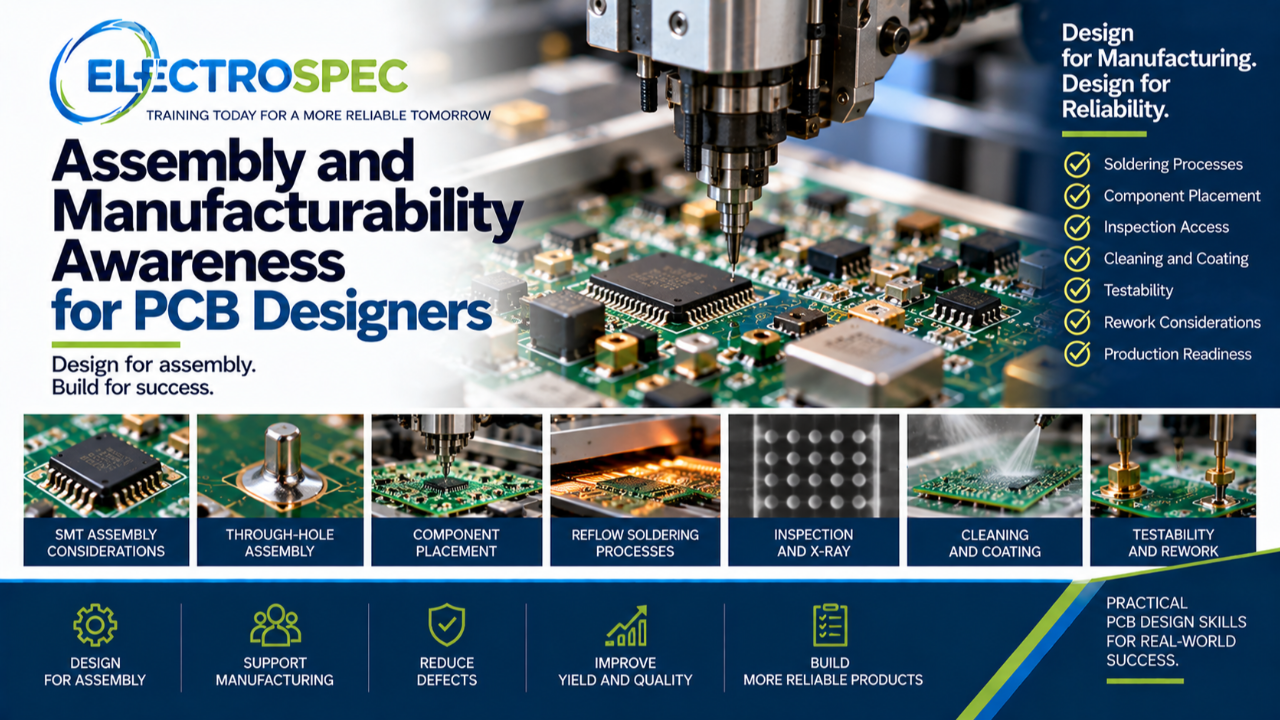
A PCB design does not succeed only because the circuit is correct.
It must also be assembled.
That means the board must support component placement, soldering, cleaning, coating, inspection, test, handling, and rework when allowed.
A layout that ignores assembly can create avoidable defects, delays, cost, and reliability problems.
That is why PCB designers need assembly and manufacturability awareness.
Assembly Process Matters
Different products use different assembly processes.
A design may involve SMT reflow, through-hole assembly, wave soldering, selective soldering, manual soldering, robotic soldering, press-fit installation, cleaning, conformal coating, staking, bonding, or special handling.
The designer should understand which process will be used.
The process should influence land patterns, spacing, orientation, thermal relief, component placement, test access, inspection access, and documentation.
SMT Layout Needs Process Awareness
SMT assembly depends on paste printing, component placement, reflow, solder joint formation, inspection, and sometimes rework.
Designers should consider pad design, stencil needs, component spacing, thermal balance, package type, tombstoning risk, solder bridging risk, bottom termination inspection, and reflow profile sensitivity.
A good SMT layout supports the process.
Through-Hole Design Also Needs Process Awareness
Through-hole assembly may use wave soldering, selective soldering, manual soldering, or other methods.
Designers should consider hole-to-lead relationship, pad size, annular ring, thermal relief, board thickness, solder fill, component clearance, and inspection access.
Through-hole reliability is affected by both design and process.
Inspection Access Must Be Designed
Manufacturability includes inspection.
Designers should ask whether solder joints can be viewed, whether polarity marks remain visible, whether reference designators are useful, whether X-ray inspection is required, and whether coating or cleanliness can be verified.
If inspection cannot confirm product quality, acceptance becomes more difficult.
Cleaning and Coating Affect Layout
Cleaning access and coating strategy should be considered before release.
Dense components, low standoff packages, trapped flux areas, connectors, test points, and coating keep-outs can all affect process success.
Conformal coating does not fix poor layout.
The design must support cleaning, coating, inspection, and documentation.
Testability Is Part of Manufacturability
A product that cannot be tested efficiently may create production delays and weak evidence.
Designers should consider test points, programming access, connectors, boundary scan, functional test, fixture access, environmental test monitoring, and troubleshooting.
Test access should be designed in, not added at the end.
Rework Should Not Be the Plan
Rework may be necessary sometimes, but it should not be the default manufacturing strategy.
Repeated rework can increase cost, schedule risk, and reliability concerns.
Designers should consider whether rework is possible, allowed, accessible, and controlled.
A layout that requires frequent rework should be reviewed.
Manufacturability Must Be Reviewed Early
Manufacturability review should happen before release.
Designers should involve process engineering, manufacturing, inspection, test, quality, and suppliers when appropriate.
A good review asks whether the product can be built, inspected, tested, accepted, documented, and trusted.
CID Builds Manufacturing Awareness
ElectroSpec’s CID Fundamentals course includes manufacturability because designers need to understand how layout decisions affect assembly and production.
The course provides 22+ hours of self-paced, on-demand PCB design training across 12 structured modules covering materials, layout principles, mechanical and electrical considerations, thermal management, component technologies, interconnections, fabrication requirements, documentation, quality assurance, manufacturability, and standards-based design thinking.
Final Thought
Manufacturability is not a separate department’s problem.
It starts in design.
PCB designers influence soldering, assembly, inspection, cleaning, coating, testability, rework, reliability, documentation, and product acceptance.
A strong designer does not only ask, “Can I route it?”
A strong designer asks, “Can we build it well?”
Related ElectroSpec Training
ElectroSpec’s CID Fundamentals course provides 22+ hours of self-paced, on-demand PCB design training across 12 structured modules.
The course helps designers build a standards-connected foundation in manufacturability, layout, materials, fabrication, documentation, quality, and design decision-making while preparing for CID certification.
Coming Next
Documentation and Release Packages: Communicating Design Intent
In the next article, we will continue the CID Fundamentals track and discuss why drawings, notes, BOMs, standards callouts, release files, inspection requirements, and test requirements must clearly communicate design intent.