Designing for Environmental Stress, Qualification, and Harsh Environments
Aug 22, 2026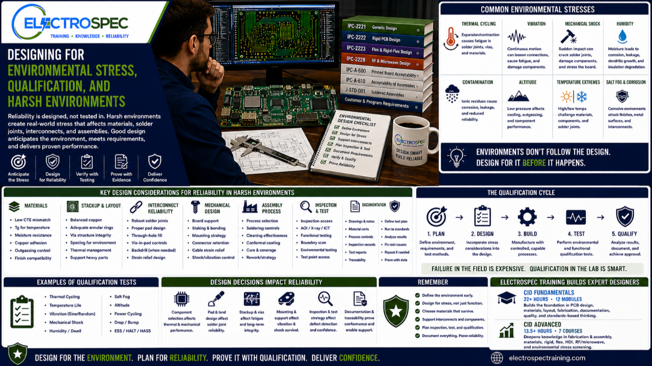
Electronics do not operate in a perfect world.
They may be exposed to heat, cold, vibration, shock, humidity, contamination, corrosion, altitude, handling damage, transportation stress, storage conditions, and long service life.
A product may pass electrical test at room temperature and still fail in the real world.
That is why environmental stress and qualification must be considered early in design.
A designer cannot wait until the product is built to think about the environment.
By then, many reliability risks may already be locked into the materials, layout, stackup, solder joints, connectors, coating strategy, mechanical support, and documentation.
Good harsh-environment design begins before release.
Harsh Environment Must Be Defined
“Harsh environment” sounds serious, but it is not a requirement by itself.
The designer must define what harsh means for the product.
Does the product face:
- thermal cycling?
- high temperature?
- low temperature?
- vibration?
- mechanical shock?
- humidity?
- condensation?
- salt fog?
- contamination?
- corrosion?
- altitude?
- pressure change?
- fluid exposure?
- storage stress?
- transportation stress?
- repeated handling?
- long mission life?
- operation on demand?
Each condition affects the design differently.
A board designed for vibration may need different mechanical support than a board designed for high humidity.
A product designed for thermal cycling may need different material and interconnect decisions than a product designed for controlled indoor use.
The environment must be translated into engineering requirements.
Qualification Is Not a Final Exam You Study for Later
Qualification testing is sometimes treated as something that happens at the end of development.
That is risky.
Qualification should influence the design from the beginning.
If a product must survive shock, vibration, thermal cycling, humidity, altitude, or other environmental conditions, those conditions should affect early design decisions.
Qualification requirements may influence:
- material selection
- laminate choice
- copper thickness
- stackup
- via structures
- component selection
- component placement
- solder joint geometry
- connector support
- board mounting
- mechanical reinforcement
- conformal coating
- cleanliness requirements
- test access
- inspection access
- documentation
- process control
A product that fails qualification may need redesign, retest, schedule recovery, customer explanation, and additional cost.
Designing for qualification early reduces that risk.
Environmental Stress Screening Is a Design Concern
Environmental Stress Screening, often called ESS, is used to expose products to controlled stresses that may reveal workmanship, process, or latent defects.
But ESS should not be viewed only as a production or test activity.
Designers need to understand what environmental stress can reveal.
Stress can expose weaknesses in:
- solder joints
- plated through-holes
- vias
- microvias
- component terminations
- connectors
- cables
- mechanical supports
- coatings
- material interfaces
- board mounting
- thermal paths
- process controls
If the design is fragile, ESS may reveal failures that were designed into the product.
That is why ElectroSpec includes Environmental Stress Screening in CID Advanced training.
Designers should understand how environmental stress connects design decisions to real-world reliability.
Thermal Cycling Drives Material and Interconnect Risk
Thermal cycling is one of the most important reliability concerns in electronics.
As temperature changes, materials expand and contract.
Different materials expand at different rates.
That mismatch can create stress.
Thermal cycling can affect:
- solder joints
- plated through-holes
- vias
- microvias
- component packages
- laminate systems
- copper interfaces
- connectors
- conformal coating
- mechanical attachments
Designers should consider coefficient of thermal expansion, material compatibility, board thickness, component package selection, solder joint geometry, mounting methods, and thermal paths.
A product that looks good at room temperature may fail after repeated temperature changes.
The designer must think about thermal behavior before the product is built.
Vibration and Shock Affect Mechanical Design
Vibration and shock are not only mechanical engineering concerns.
They affect PCB design directly.
A board that experiences vibration or shock may suffer from:
- solder joint fatigue
- component lead fatigue
- connector movement
- board flexure
- cracked components
- cracked solder joints
- fretting at contacts
- mounting failures
- cable strain
- intermittent connections
- mechanical damage
Designers should consider component mass, component height, board support, mounting hole placement, connector retention, staking, bonding, strain relief, and cable routing.
Large components, tall components, unsupported connectors, and heavy devices may need special attention.
A reliable design does not assume the board will remain perfectly still.
Humidity, Contamination, and Cleanliness Matter
Humidity and contamination can create serious reliability problems.
Moisture, ionic contamination, residues, and environmental exposure can contribute to corrosion, leakage current, dendritic growth, reduced insulation resistance, coating failures, and intermittent electrical behavior.
Designers influence humidity and contamination risk through:
- component spacing
- board density
- package selection
- bottom termination components
- cleaning access
- coating access
- solder mask design
- high-voltage spacing
- material compatibility
- flux entrapment risk
- documentation
- inspection strategy
Cleanliness is not only a production concern.
Designers can either support cleaning and verification or make them difficult.
For high-reliability products, cleanliness must be considered as part of the design strategy.
Conformal Coating Is Not a Substitute for Good Design
Conformal coating can help protect electronics from moisture, contamination, and environmental exposure.
But coating is not magic.
It does not fix poor design.
It does not remove contamination by itself.
It does not compensate for incompatible materials.
It does not solve poor spacing.
It does not eliminate the need for process control.
Designers should consider:
- coating material compatibility
- coating thickness
- masking requirements
- connector keep-outs
- test point access
- inspection method
- rework impact
- cleaning before coating
- component coverage
- sharp edges and shadowed areas
- environmental exposure
Coating should be planned early.
If coating is added late, it may conflict with inspection, test, connectors, rework, or product function.
Materials Must Match the Environment
Material selection is one of the most important design decisions for harsh environments.
Designers should consider how materials respond to:
- temperature
- moisture
- thermal cycling
- vibration
- chemical exposure
- mechanical stress
- soldering temperatures
- storage conditions
- long service life
Materials affect dielectric performance, dimensional stability, solderability, copper adhesion, plating reliability, moisture absorption, thermal expansion, coating compatibility, and long-term performance.
For Class 3, aerospace, defense, space, medical, industrial, and harsh-environment products, material selection should be intentional and traceable.
The material system is part of the reliability system.
Fabrication and Assembly Must Support Qualification
Qualification success does not depend on design alone.
The design must be supported by fabrication and assembly processes capable of meeting the requirement.
Designers should ask:
- Can the board supplier build the stackup reliably?
- Are via structures appropriate for the environment?
- Are plating requirements adequate?
- Is the surface finish compatible with assembly and reliability?
- Can the assembly process form consistent solder joints?
- Can the product be cleaned properly?
- Can coating be applied and inspected?
- Can mechanical supports be installed consistently?
- Can process controls be documented?
- Can objective evidence be produced?
A design that cannot be manufactured consistently will struggle in qualification and field use.
Inspection and Test Must Be Planned
Harsh-environment and high-reliability products need verification.
Designers should plan for inspection and test early.
That may include:
- visual inspection access
- X-ray inspection
- automated optical inspection
- in-circuit test
- functional test
- boundary scan
- programming access
- environmental test monitoring
- failure analysis access
- coating inspection
- cleanliness verification
- connector inspection
- mechanical support verification
A design that cannot be inspected or tested with confidence creates acceptance risk.
If the design requires hidden solder joints, dense packaging, coating, staking, or special environmental verification, the inspection and test strategy should be defined before release.
Documentation Turns Requirements Into Evidence
For high-reliability products, documentation is part of the design.
Documentation may include:
- drawings
- material specifications
- fabrication notes
- assembly notes
- inspection requirements
- test requirements
- coating requirements
- cleaning requirements
- qualification requirements
- environmental requirements
- process controls
- acceptance criteria
- objective evidence records
A requirement that is not clearly documented may not be properly implemented.
A design decision that is not traceable may be difficult to defend later.
Documentation helps connect the design to manufacturing, inspection, test, qualification, and customer acceptance.
Standards Traceability Matters
Environmental and qualification requirements should be traceable.
The designer should know where each requirement comes from.
It may come from:
- customer drawings
- contracts
- purchase orders
- IPC standards
- Class 3 requirements
- NASA requirements
- ESA requirements
- military specifications
- IEC standards
- company design rules
- qualification plans
- environmental test plans
- engineering analysis
- supplier capability
- customer flow-downs
Traceability helps designers understand what is mandatory, what is recommended, what is supplier capability, and what is engineering judgment.
That matters when the design is reviewed, audited, qualified, or investigated after a failure.
CID Advanced Connects Environmental Stress to Design
ElectroSpec CID Advanced includes Environmental Stress Screening because designers need to understand how stress affects real products.
The advanced track also includes:
- PCB Fabrication & Assembly
- PCB Materials
- Rigid PCB Design
- Flexible PCB Design
- HDI PCB Design
- RF/Microwave PCB Design
- Environmental Stress Screening
These topics work together.
Environmental reliability depends on materials, fabrication, assembly, board technology, interconnect design, inspection, testing, and documentation.
A designer cannot separate environmental performance from the rest of the design system.
That is why CID Advanced is built as a connected advanced design pathway.
CID Fundamentals Builds the Base
ElectroSpec CID Fundamentals provides the design foundation needed before advanced topics make sense.
The course includes 22+ hours of on-demand training across 12 structured modules covering materials, layout principles, mechanical and electrical considerations, thermal management, component technologies, interconnections, fabrication requirements, documentation, quality assurance, manufacturability, and standards-based design thinking.
A designer preparing for harsh-environment products needs that foundation first.
Advanced reliability depends on basic design discipline.
Environmental Design Still Requires Judgment
Standards and qualification plans provide requirements.
But designers still need judgment.
They must balance:
- reliability and cost
- performance and manufacturability
- density and inspection access
- material performance and availability
- environmental risk and schedule
- test coverage and design complexity
- coating protection and rework access
- customer requirements and supplier capability
There is rarely one perfect answer.
The designer must understand the requirements, evaluate the risks, and make a defensible design decision.
Standards provide the rules.
Designers create the solution.
A Better Environmental Design Review
A strong environmental design review should ask:
- What environment must the product survive?
- What qualification tests apply?
- What standards and specifications are invoked?
- What class applies?
- What customer flow-downs apply?
- Are the materials appropriate?
- Can the stackup survive the environment?
- Are solder joints and interconnects protected from fatigue?
- Are connectors and cables supported?
- Can the product be cleaned and coated?
- Can the product be inspected and tested?
- What objective evidence will prove conformance?
- What failure modes should be reviewed before release?
These questions help designers prevent problems before they become qualification failures.
Independently Developed by ElectroSpec
ElectroSpec’s CID and CID Advanced courses are independently developed by ElectroSpec.
They are not IPC-authorized training and they are not official IPC curriculum.
ElectroSpec developed these courses to provide practical, standards-connected, manufacturing-aware design training for students preparing for CID and CID+ certification.
The focus is not only on knowing design rules.
The focus is on understanding how design decisions affect reliability in real environments.
Final Thought
Harsh-environment reliability is not created at final test.
Qualification success is not created after the product is built.
Environmental performance begins in design.
The designer must understand the product environment, applicable standards, material behavior, fabrication capability, assembly process, inspection strategy, test plan, qualification requirements, and objective evidence.
A product that survives the real world is not lucky.
It is designed, built, tested, verified, and documented with purpose.
That is the mindset designers need.
Related ElectroSpec Training
ElectroSpec’s CID Fundamentals course provides 22+ hours of on-demand PCB design training across 12 structured modules.
ElectroSpec’s CID Advanced training expands into PCB Fabrication & Assembly, PCB Materials, Rigid PCB Design, Flexible PCB Design, HDI PCB Design, RF/Microwave PCB Design, and Environmental Stress Screening.
Together, these courses help designers build the standards-connected foundation needed for CID and CID+ certification preparation.
Coming Next
The Designer as Engineer and Artist: Standards Give the Rules, Creativity Builds the Product
In the final article of this series, we will discuss how standards provide the rules and constraints, but the designer brings creativity, experience, judgment, and talent to create the final product.
IPC CID Certification — ElectroSpec
IPC CID+ Certification — ElectroSpec
IPC CID/CID+ Bundle — Complete PCB Design Certification — ElectroSpec