Environmental Stress Screening: Designing for the Real World
Sep 21, 2026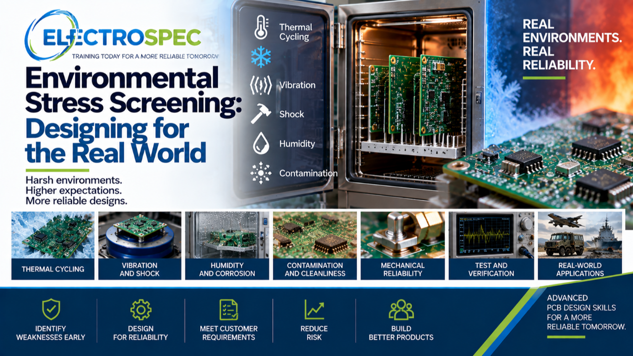
Products do not operate in perfect conditions.
They may experience shock, vibration, thermal cycling, humidity, contamination, storage, transportation, handling, power cycling, and long service life.
A product may pass electrical test and still fail when exposed to the real world.
That is why environmental stress screening and qualification thinking matter for advanced PCB designers.
ESS is not only a production or test topic.
It is a design topic.
Stress Reveals Weakness
Environmental stress can reveal weaknesses in design, materials, fabrication, assembly, solder joints, connectors, coatings, mechanical support, and process control.
Stress may expose:
- cracked solder joints
- weak vias
- microvia failures
- connector movement
- poor component support
- coating defects
- cleanliness issues
- thermal mismatch
- board flexure
- intermittent connections
If the design is fragile, stress may reveal the fragility.
Designers Should Understand the Environment
Before release, designers should understand what the product must survive.
- Will it see thermal cycling?
- Will it experience vibration?
- Will it be transported long distances?
- Will it operate in humidity?
- Will it be stored for long periods?
- Will it be used in aerospace, defense, medical, industrial, or harsh-environment applications?
The environment should shape material selection, stackup, component placement, solder joint strategy, connector support, coating, cleanliness, inspection, test, and qualification planning.
Thermal Cycling Is a Major Reliability Driver
Thermal cycling stresses materials because different materials expand and contract at different rates.
This can affect solder joints, plated through-holes, vias, microvias, component packages, laminate structures, and coatings.
Designers should consider coefficient of thermal expansion, material compatibility, board thickness, copper distribution, component package selection, and interconnect reliability.
A board that works at room temperature may not survive repeated thermal cycling.
Vibration and Shock Affect the Layout
Vibration and shock can damage solder joints, components, connectors, cables, and board supports.
Designers should consider component mass, connector retention, board mounting, stiffening, support points, staking or bonding, cable strain relief, and service handling.
A product exposed to vibration needs mechanical awareness in the PCB layout.
Humidity and Contamination Affect Reliability
Humidity and contamination can create corrosion, leakage current, dendritic growth, insulation resistance problems, coating failure, and intermittent behavior.
Designers affect cleanliness and contamination risk through spacing, component density, package choice, cleaning access, coating strategy, solder mask, and documentation.
Cleanliness is not only a production issue. Design can either support it or make it difficult.
Coating Is Not a Magic Fix
Conformal coating can help protect electronics, but it does not repair poor design.
Designers should plan coating requirements early, including material compatibility, keep-outs, masking, thickness, coverage, inspection, rework, cleaning, and environmental exposure.
Coating works best when the design supports coating.
ESS Must Be Connected to Requirements
Environmental stress screening should be tied to requirements and risk.
Designers should understand what the stress is intended to reveal and what evidence is required.
Stress without purpose can waste time.
Stress connected to requirements can build confidence.
The designer should know how ESS relates to qualification, production screening, reliability improvement, and objective evidence.
Test and Inspection Must Be Planned
Environmental testing may require monitoring points, connectors, fixtures, diagnostic access, visual inspection, X-ray inspection, functional test, or failure analysis access.
Designers should plan for verification before the product is built.
A product that cannot be monitored or diagnosed during testing may be difficult to improve after failure.
CID Advanced Builds Environmental Thinking
ElectroSpec’s CID Advanced track includes Environmental Stress Screening because advanced designers need to understand how real-world stress affects PCB reliability.
ESS connects directly to materials, fabrication, assembly, interconnections, mechanical support, inspection, test, documentation, and qualification.
It is part of the larger CID Advanced pathway, which also includes PCB Fabrication & Assembly, PCB Materials, Rigid PCB Design, Flexible PCB Design, HDI PCB Design, and RF/Microwave PCB Design.
Final Thought
Environmental stress screening is not just something done after design.
It is a reminder that the product must survive real use.
Shock, vibration, thermal cycling, humidity, contamination, handling, and long service life should influence design decisions early.
A strong advanced designer does not only design for first power-up.
A strong designer designs for the real world.
Related ElectroSpec Training
ElectroSpec’s CID Advanced training includes Environmental Stress Screening as part of a specialized advanced PCB design pathway.
The CID Advanced track also includes PCB Fabrication & Assembly, PCB Materials, Rigid PCB Design, Flexible PCB Design, HDI PCB Design, and RF/Microwave PCB Design.
Together, these courses help designers build the advanced reliability awareness needed for CID+ certification preparation and real-world design decisions.
Coming Next
Fabrication Requirements Every PCB Designer Should Understand
In the next article, we will return to the CID Fundamentals track and discuss why fabrication requirements affect every board, from materials and copper to holes, solder mask, surface finish, tolerances, inspection, and supplier communication.