Fabrication Requirements Every PCB Designer Should Understand
Sep 22, 2026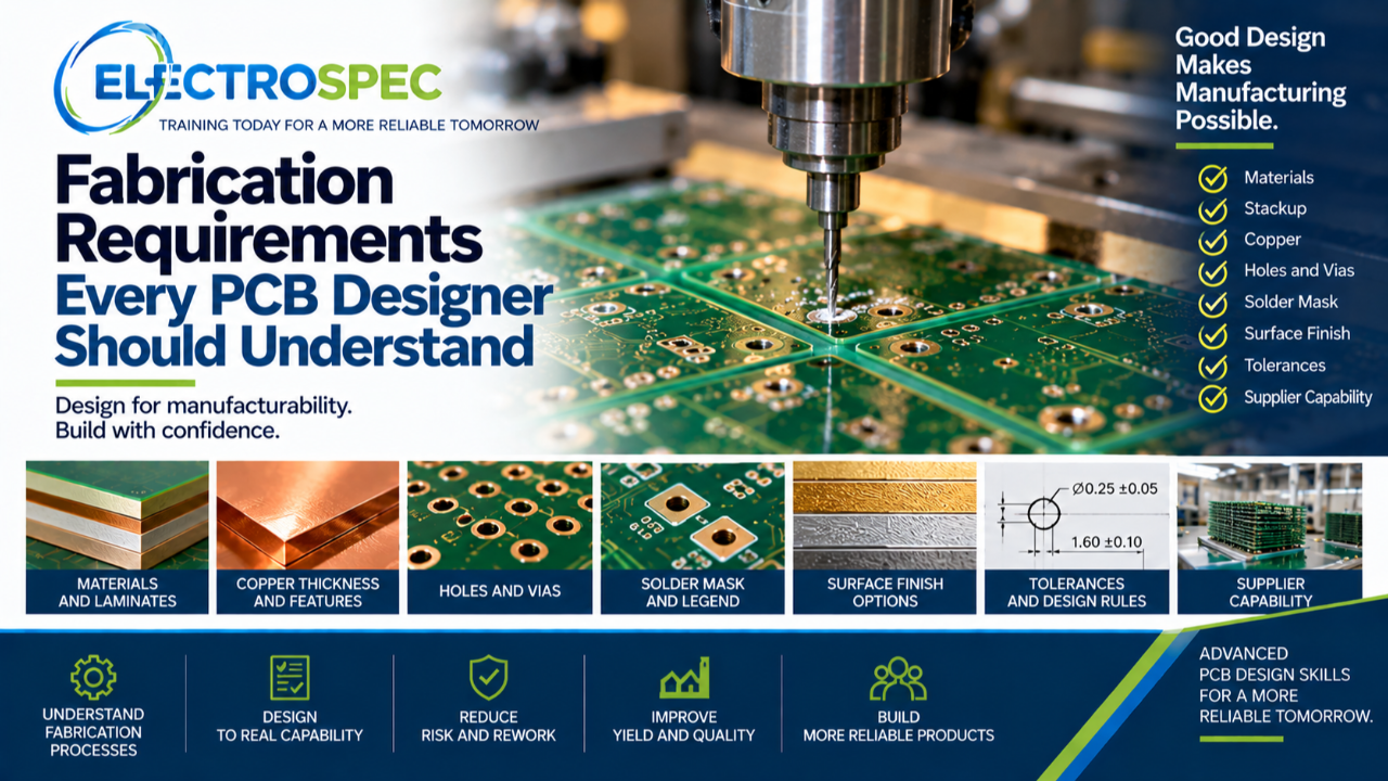
PCB designers do not fabricate the board.
But their decisions determine whether the board can be fabricated reliably.
A design may be electrically correct, but if fabrication requirements are unclear, unrealistic, incomplete, or poorly communicated, the product can run into supplier holds, yield problems, inspection issues, rework, delays, or reliability concerns.
That is why PCB designers must understand fabrication requirements.
Fabrication Turns Design Into Hardware
Fabrication is where the board becomes physical.
The fabricator must build the board using the drawings, data files, stackup, material requirements, copper features, holes, vias, solder mask, surface finish, tolerances, and inspection requirements supplied by the design team.
If the design package is unclear, the fabricator must ask questions or make assumptions.
Good PCB design reduces unnecessary assumptions.
Materials Must Be Defined
Material requirements matter because the material system affects electrical performance, thermal behavior, soldering, dimensional stability, moisture resistance, fabrication yield, and reliability.
Designers should understand whether the material is common, controlled, high Tg, low loss, flexible, RF-focused, HDI-suitable, or tied to customer requirements.
Material requirements should be clear enough for purchasing, fabrication, inspection, and objective evidence.
Stackup Must Be Realistic
Stackup affects fabrication, impedance, power distribution, signal performance, thermal behavior, mechanical stiffness, and cost.
Designers should define the layer structure, dielectric thickness, copper weights, material system, reference planes, controlled impedance needs, and supplier capability.
A stackup should not be copied blindly from another product.
It should fit the current design.
Copper Thickness Affects Fabrication
Copper thickness affects current capacity, etching, spacing, impedance, thermal behavior, soldering, and cost.
Heavier copper may support current and heat spreading, but it can make fine features more difficult.
Thinner copper may support fine routing, but it may not meet current or reliability needs.
Copper selection must match the product requirement.
Holes and Vias Must Be Buildable
Holes and vias are fabricated structures.
Designers should consider drill size, finished hole size, plating, aspect ratio, annular ring, tolerances, via structures, lead fit, and inspection.
For more advanced designs, blind vias, buried vias, microvias, and via-in-pad features require even stronger supplier review.
A hole is not just a hole. It is part of the interconnect reliability system.
Solder Mask and Surface Finish Matter
Solder mask affects soldering, bridging risk, exposed copper, inspection visibility, cleaning, coating, and fabrication registration.
Surface finish affects solderability, shelf life, planarity, corrosion risk, contact performance, assembly compatibility, and reliability.
These should not be last-minute choices.
They are fabrication requirements with assembly and reliability consequences.
Tolerances Should Be Intentional
Tolerances define what variation is acceptable.
Designers should consider board outline tolerances, hole tolerances, thickness tolerances, slot and cutout tolerances, controlled impedance tolerance, and mechanical interface requirements.
Overly tight tolerances can increase cost and reduce yield.
Overly loose tolerances can create fit, assembly, or performance problems.
Good tolerance selection requires judgment.
Supplier Capability Must Be Reviewed
Supplier capability affects what can be built consistently.
Designers should review minimum line width, spacing, drill size, aspect ratio, copper thickness, layer count, materials, solder mask registration, surface finish, impedance control, HDI capability, flex capability, inspection capability, and lead time.
A design rule is only useful if it is tied to real capability and real requirements.
Documentation Must Communicate Clearly
Fabrication documentation may include drawings, notes, stackup, hole tables, material callouts, copper requirements, solder mask notes, surface finish, standards, product class, inspection requirements, impedance requirements, test requirements, and special instructions.
Good documentation turns design intent into build instruction.
Poor documentation creates guesswork.
CID Builds Fabrication Awareness
ElectroSpec’s CID Fundamentals course includes fabrication requirements because designers need to understand how layout decisions affect the board supplier.
The course provides 22+ hours of self-paced, on-demand PCB design training across 12 structured modules covering materials, layout principles, mechanical and electrical considerations, thermal management, component technologies, interconnections, fabrication requirements, documentation, quality assurance, manufacturability, and standards-based design thinking.
Final Thought
Fabrication requirements are not somebody else’s problem.
They are part of PCB design.
Materials, stackup, copper, holes, vias, solder mask, surface finish, tolerances, inspection, and supplier capability all affect whether the board can be built and trusted.
A strong designer understands fabrication before release.
Related ElectroSpec Training
ElectroSpec’s CID Fundamentals course provides 22+ hours of self-paced, on-demand PCB design training across 12 structured modules.
The course helps designers build a standards-connected foundation in materials, layout, fabrication requirements, documentation, manufacturability, quality, and design decision-making while preparing for CID certification.
Coming Next
Assembly and Manufacturability Awareness for PCB Designers
In the next article, we will continue the CID Fundamentals track and discuss why designers must understand how layout decisions affect soldering, assembly processes, inspection access, cleaning, coating, test, rework, and production readiness.