PCB Fabrication and Materials: Why Designers Need Traceability Back to Standards
Aug 06, 2026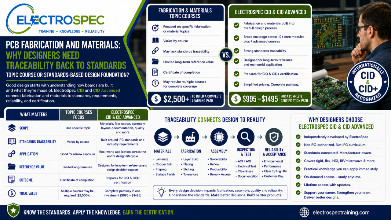
PCB fabrication and materials are not background topics.
They are design topics.
A designer may create the schematic and layout, but the final product depends on how the bare printed board is fabricated, what materials are selected, how copper is formed, how vias are plated, how solder mask is applied, how surface finishes are specified, and how the board survives assembly and real-world use.
That is why fabrication and materials training matters.
But when comparing PCB design courses, buyers should ask an important question:
Is fabrication and materials training being taught as a standalone topic, or is it connected back to the standards, design requirements, manufacturing process, quality expectations, and certification pathway that designers need?
That distinction matters.
A fabrication overview may explain how boards are made.
A standards-based design pathway helps the designer understand how fabrication and material choices affect reliability, manufacturability, inspection, acceptance, and long-term product performance.
Fabrication Is Where the Design Becomes Physical
The PCB layout is not the product.
The fabricated board is where the design starts becoming physical.
Every design decision eventually has to survive the board fabrication process.
That includes:
- laminate selection
- resin system
- glass reinforcement
- copper thickness
- conductor width
- conductor spacing
- plated through-holes
- via structures
- annular ring
- board thickness
- layer count
- stackup
- impedance control
- solder mask
- surface finish
- marking
- panelization
- tolerances
- documentation
- inspection requirements
These are not just board shop concerns.
They are designer concerns.
A designer who does not understand fabrication may create requirements that are difficult, expensive, unreliable, or impossible to build consistently.
Materials Drive Reliability
Materials are not just purchasing choices.
Materials influence electrical performance, thermal behavior, mechanical strength, soldering performance, moisture absorption, dimensional stability, and long-term reliability.
A designer should understand how material choices affect:
- dielectric performance
- thermal expansion
- glass transition behavior
- copper adhesion
- plating reliability
- solderability
- impedance control
- flexural behavior
- chemical compatibility
- cleaning compatibility
- conformal coating compatibility
- moisture sensitivity
- high-temperature performance
- vibration and mechanical stress
- Class 3 or high-reliability expectations
Material selection is especially important for aerospace, defense, medical, industrial, RF, microwave, high-speed, flex, HDI, and harsh-environment products.
A low-risk consumer product and a high-reliability Class 3 product may not require the same material decisions.
The designer must understand the difference.
The Topic Course Approach
Based on the catalog descriptions reviewed, fabrication-related PCB design courses may be offered as individual topic courses.
Those courses can be useful.
A student may learn how boards are fabricated, what suppliers need, how fabrication issues occur, or how emerging technologies affect PCB design.
That can help designers communicate better with fabrication suppliers.
But there is a limitation.
A standalone fabrication topic course may not provide the complete standards-based framework needed to connect fabrication decisions to design requirements, material standards, assembly processes, inspection, acceptance criteria, environmental reliability, and certification preparation.
Fabrication is not isolated from the rest of the design.
It is connected to nearly everything.
ElectroSpec CID Covers Fabrication as Part of the Foundation
ElectroSpec’s CID Fundamentals course is a 22+ hour on-demand PCB Fundamentals Course with 12 structured modules.
The course covers materials, layout principles, mechanical and electrical considerations, thermal management, component technologies, interconnections, fabrication requirements, documentation, and quality assurance.
Fabrication is not treated as a quick overview.
It is part of the full design foundation.
That matters because designers need to understand how fabrication requirements connect to layout, materials, documentation, quality, and reliability.
For example:
A conductor spacing decision may affect electrical safety, manufacturability, and inspection.
A via decision may affect fabrication yield and long-term reliability.
A solder mask decision may affect assembly, solder joint formation, and inspection.
A surface finish decision may affect solderability, shelf life, cost, and reliability.
A material decision may affect thermal cycling, moisture exposure, impedance, and mechanical stability.
These are design decisions, not just fabrication details.
ElectroSpec CID Advanced Expands Fabrication and Materials
ElectroSpec’s CID Advanced training goes deeper.
The advanced track includes:
- PCB Fabrication & Assembly, 4.5 hours
- PCB Materials, 1.75 hours
- Rigid PCB Design, 1 hour
- Flexible PCB Design, 1 hour
- HDI PCB Design, 1.5 hours
- RF/Microwave PCB Design, 1.75 hours
- Environmental Stress Screening, 2 hours
This is important because fabrication and materials do not affect every board the same way.
Rigid boards, flex circuits, HDI designs, RF/microwave products, and harsh-environment assemblies each introduce different fabrication and material concerns.
A designer needs to understand how those areas connect.
That is why ElectroSpec does not treat fabrication and materials as isolated topics.
They are part of a broader advanced design pathway.
Standards Traceability Is the Key Difference
Fabrication and materials training should help the designer trace information back to the right source.
A designer should be able to ask:
- Is this a generic design requirement?
- Is this a rigid board requirement?
- Is this a flex or rigid-flex requirement?
- Is this related to RF or microwave performance?
- Is this tied to a material specification?
- Is this tied to bare board acceptability?
- Is this tied to solderability?
- Is this tied to solder mask requirements?
- Is this tied to conformal coating compatibility?
- Is this tied to marking or identification?
- Is this tied to assembly requirements?
- Is this tied to Class 3 reliability expectations?
- Is this tied to the customer drawing or contract?
- Is this tied to environmental qualification?
That is standards traceability.
Without traceability, designers may remember advice without understanding its technical basis.
With traceability, designers can make better decisions, communicate with suppliers, defend design choices, and support objective evidence.
Supporting Standards Matter
PCB design is not governed by one document.
A designer may need to understand how design requirements connect to many supporting standards and material requirements.
Examples include areas such as:
- generic printed board design requirements
- rigid printed board design
- flexible and rigid-flex design
- RF and high-frequency design
- bare board performance and acceptability
- laminate and prepreg materials
- copper foil
- solder mask
- surface finishes
- marking and identification
- solderability
- soldering materials
- fluxes
- solder pastes
- conformal coating
- cleanliness and process compatibility
The specific standard depends on the product, technology, customer, contract, drawing, and intended environment.
That is exactly why designers need a standards-based framework.
They need to know where to look and how the pieces connect.
Courses Come and Go, But Standards Remain the Reference Point
Training catalogs change.
Course titles are renamed.
Topics are repackaged.
New offerings appear, and older offerings may disappear.
That is normal.
But fabrication and material requirements do not disappear just because a course catalog changes.
Designers still need a durable reference framework.
They need to understand how to return to the standards, drawings, specifications, and requirements that govern the product.
This matters because real PCB design work often requires later review.
A design may be questioned by a supplier, process engineer, inspector, quality engineer, customer, auditor, or failure analysis team.
When that happens, the designer should be able to explain the design decision and connect it back to the requirement.
That is why reference value matters.
Certificate of Completion vs. Certification Preparation
A standalone fabrication or materials course may provide a certificate of completion.
That can document that the student completed the class.
But completion is not the same as a certification pathway.
ElectroSpec’s CID and CID Advanced courses are built to support preparation for CID and CID+ certification.
That means the training is not only about learning fabrication terminology.
It is about helping the designer build a broader foundation tied to recognized PCB design certification goals.
For employers, customers, and technical managers, that distinction matters.
A certificate of completion may show exposure.
CID and CID+ preparation supports a broader professional design credential.
Price and Value
Price should be compared to scope, reference value, and outcome.
A single fabrication topic course may be a good fit for someone who only needs limited exposure.
But a designer trying to build a complete learning path may need more than one course.
They may need training in materials, fabrication, assembly, rigid board design, flex, HDI, RF, manufacturability, quality, inspection, and reliability.
Those separate topic costs can add up quickly.
ElectroSpec’s simplified comparison is different.
ElectroSpec CID and CID Advanced are commonly positioned in the $995 to $1,495 range, depending on the offering.
A broader pathway built from multiple individual topic courses can reach $2,500+.
The better question is:
Is the student buying one topic, or building a standards-based pathway toward certification?
Comparison Summary
| Question | Fabrication or Materials Topic Course | ElectroSpec CID and CID Advanced |
|---|---|---|
| Main purpose | Teach selected fabrication or material concepts | Build fabrication and materials into a broader design framework |
| Scope | Course dependent | Materials, fabrication, assembly, layout, documentation, quality, reliability |
| Standards traceability | Varies by course | Built around standards and requirements |
| Reference value | May be limited to one topic | Designed for long-term reference and real project application |
| Advanced coverage | May require multiple separate courses | Includes fabrication, materials, rigid, flex, HDI, RF/microwave, and ESS |
| Outcome | Often certificate of completion | Supports CID and CID+ certification preparation |
| Best fit | Narrow topic exposure | Designers seeking a standards-based certification pathway |
Designers Need to Understand the Board Before They Design the Board
A PCB designer should not think of fabrication as something that happens after design.
Fabrication capability should influence the design from the beginning.
The designer should understand:
- Can this stackup be built reliably?
- Are the material selections appropriate?
- Are the conductor widths and spacings manufacturable?
- Are the holes and vias reasonable for the fabrication process?
- Are the tolerances clearly documented?
- Is the solder mask strategy appropriate?
- Is the surface finish compatible with assembly and reliability?
- Are the fabrication notes clear?
- Can the supplier inspect and verify the requirements?
- Does the design support the intended product class?
- Does the design support the operating environment?
These questions belong in design review before the board is released.
Independently Developed by ElectroSpec
ElectroSpec’s CID and CID Advanced courses are independently developed by ElectroSpec.
They are not IPC-authorized training and they are not official IPC curriculum.
ElectroSpec built these courses to provide practical, standards-connected, manufacturing-aware training for designers pursuing CID and CID+ certification preparation.
The focus is not only on what the standards say.
The focus is on how designers apply the requirements in real products.
Final Thought
PCB fabrication and materials are not secondary topics.
They are central to PCB design.
A designer who understands fabrication and materials can make better decisions about stackup, layout, tolerances, documentation, solderability, reliability, supplier capability, and product acceptance.
A topic course may teach selected fabrication concepts.
ElectroSpec CID and CID Advanced help designers connect fabrication and materials to the broader standards-based design framework.
That is the difference.
Fabrication explains how the board is built.
Materials explain what the board is made of.
Standards traceability explains why the design decisions matter.
Certification preparation gives the designer a professional goal.
Related ElectroSpec Training
ElectroSpec’s CID Fundamentals course provides 22+ hours of on-demand PCB design training across 12 structured modules.
ElectroSpec’s CID Advanced training includes advanced courses in PCB Fabrication & Assembly, PCB Materials, Rigid PCB Design, Flexible PCB Design, HDI PCB Design, RF/Microwave PCB Design, and Environmental Stress Screening.
Together, they provide a practical, standards-connected pathway for designers preparing for CID and CID+ certification.
Coming Next
Flex and Rigid-Flex Training: Topic Course or Advanced Design Framework?
In the next article, we will compare flex and rigid-flex topic courses with ElectroSpec’s CID Advanced approach and explain why flex design cannot be separated from materials, fabrication, mechanical stress, assembly, inspection, and reliability.
IPC CID Certification — ElectroSpec
IPC CID+ Certification — ElectroSpec
IPC CID/CID+ Bundle — Complete PCB Design Certification — ElectroSpec